In the simplest terms, deposition is the process of adding a thin layer of material onto a surface, known as a substrate. In microfabrication, this is a fundamental "building" step, where atoms or molecules are meticulously applied to a silicon wafer to construct the intricate layers that form transistors, wires, and other components of an integrated circuit.
The core concept to understand is that deposition isn't a single action but a category of highly controlled techniques. The critical choice is between two families of methods—Physical Vapor Deposition (PVD) and Chemical Vapor Deposition (CVD)—each suited for creating different types of layers with specific properties.
The Role of Deposition in Fabrication
Why Layers Are Everything
Modern microchips are not flat; they are three-dimensional structures built layer by layer, sometimes with over 100 distinct levels. Each layer serves a specific purpose.
Some layers must be conductive to act as wires (e.g., copper, aluminum). Others must be insulating to prevent electrical short circuits (e.g., silicon dioxide). Still others must be semiconducting to form the transistors themselves (e.g., polycrystalline silicon).
Deposition is the essential process used to create each of these critical films with nanometer-scale precision.
The Two Pillars: Physical vs. Chemical Deposition
The fundamental difference between the two main deposition methods lies in how the material travels from its source to the substrate.
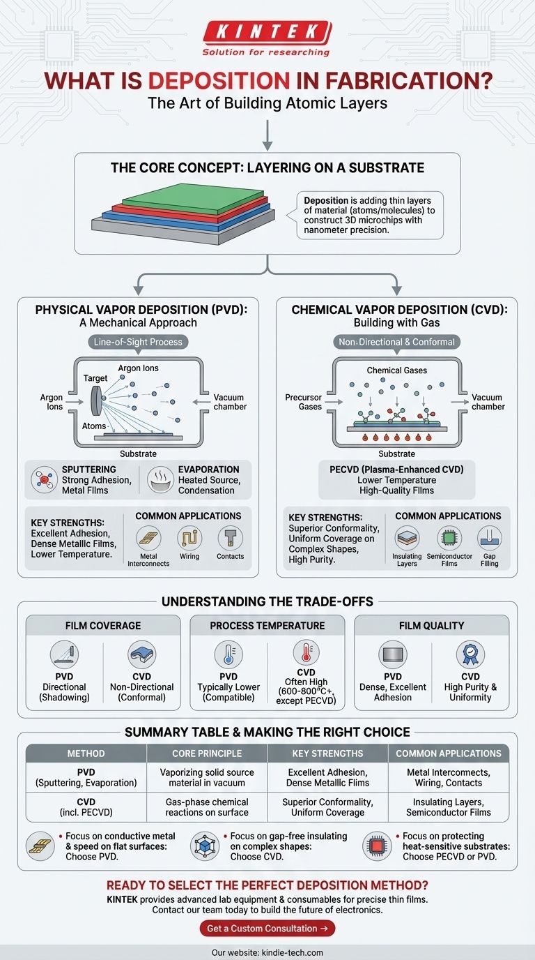
Physical Vapor Deposition (PVD): A Mechanical Approach
PVD is a line-of-sight process where a solid or liquid source material is vaporized in a vacuum and then condenses onto the substrate. Think of it like a highly controlled form of spray painting, but with individual atoms.
The two most common PVD techniques are sputtering and evaporation.
How Sputtering Works
In sputtering, a target made of the desired material is bombarded with high-energy ions (typically argon). This collision physically knocks atoms off the target, which then travel through the vacuum and coat the substrate.
Sputtering is highly valued for its strong adhesion and is a workhorse for depositing metal films used for wiring and contacts.
How Evaporation Works
Evaporation is simpler: the source material is heated in a vacuum until it turns into a gas. These gaseous atoms travel in a straight line until they hit the cooler substrate, where they condense back into a solid thin film.
While effective, this method can sometimes result in less dense films and poorer adhesion compared to sputtering.
Chemical Vapor Deposition (CVD): Building with Gas
CVD is a process where the substrate is exposed to one or more volatile precursor gases. These gases react or decompose on the substrate's surface, leaving behind the desired solid thin film.
Imagine how moisture in the air (a gas) forms a solid layer of frost on a cold window pane. CVD operates on a similar principle, but with carefully chosen chemicals to build specific materials.
The Power of Conformality
The key advantage of CVD is its conformality. Because the precursor gases can flow into and around complex surface features, CVD can deposit a film of uniform thickness over highly irregular, three-dimensional topography. This is something PVD's line-of-sight nature struggles with.
Understanding the Trade-offs
Choosing between PVD and CVD is not a matter of which is "better," but which is right for the specific task. The decision involves critical trade-offs.
Film Coverage: Line-of-Sight vs. Conformal
PVD is directional. It excels at coating the top surface of a feature but provides poor coverage on sidewalls, an effect known as shadowing.
CVD is non-directional. Its ability to uniformly coat complex shapes makes it essential for creating insulating layers that must perfectly encapsulate underlying wiring without leaving any gaps.
Process Temperature
Traditional CVD processes often require very high temperatures (600-800°C or more) to drive the necessary chemical reactions. These temperatures can damage or alter previously deposited layers.
PVD methods, especially sputtering, can typically be performed at much lower temperatures, making them compatible with a wider range of materials and fabrication steps. A variant called Plasma-Enhanced CVD (PECVD) was developed specifically to allow for high-quality film deposition at lower temperatures.
Film Purity and Quality
Both methods can produce high-quality films, but their strengths differ. CVD, particularly Low-Pressure CVD (LPCVD), is known for producing films of exceptional purity and uniformity.
PVD, on the other hand, is often preferred for creating dense metallic films with excellent adhesion, which is critical for reliable electrical interconnects.
Making the Right Choice for Your Goal
- If your primary focus is creating conductive metal interconnects on a relatively flat surface: PVD (specifically sputtering) is the industry standard due to its speed, excellent adhesion, and control over film density.
- If your primary focus is depositing a gap-free insulating layer over complex, non-planar topography: CVD is the only viable choice because of its superior conformality.
- If your primary focus is depositing a film onto a substrate with heat-sensitive components: A low-temperature method like PECVD or PVD is required to prevent damage to the underlying device.
Understanding the principles of deposition is to understand how modern electronics are fundamentally constructed, one atomic layer at a time.
Summary Table:
| Deposition Method | Core Principle | Key Strengths | Common Applications |
|---|---|---|---|
| Physical Vapor Deposition (PVD) | Vaporizing a solid source material in a vacuum. | Excellent adhesion, dense metallic films, lower temperature. | Metal interconnects, wiring, contacts. |
| Chemical Vapor Deposition (CVD) | Using gas-phase chemical reactions on the substrate. | Superior conformality, uniform coverage on complex shapes. | Insulating layers, semiconductor films. |
Ready to Select the Perfect Deposition Method for Your Project?
Choosing between PVD and CVD is critical for the performance and yield of your devices. The experts at KINTEK are here to help. We specialize in providing the advanced lab equipment and consumables you need to achieve precise, high-quality thin films.
Contact our team today to discuss your specific application, and let us help you build the future of electronics, one atomic layer at a time.
Visual Guide
Related Products
- Chemical Vapor Deposition CVD Equipment System Chamber Slide PECVD Tube Furnace with Liquid Gasifier PECVD Machine
- RF PECVD System Radio Frequency Plasma-Enhanced Chemical Vapor Deposition RF PECVD
- Inclined Rotary Plasma Enhanced Chemical Vapor Deposition PECVD Equipment Tube Furnace Machine
- Customer Made Versatile CVD Tube Furnace Chemical Vapor Deposition Chamber System Equipment
- Inclined Rotary Plasma Enhanced Chemical Vapor Deposition PECVD Equipment Tube Furnace Machine
People Also Ask
- What happens during deposition chemistry? Building Thin Films from Gaseous Precursors
- What types of substrates are used in CVD to facilitate graphene films? Optimize Graphene Growth with the Right Catalyst
- What are the processes of vapor phase deposition? Understand CVD vs. PVD for Superior Thin Films
- How are carbon nanotubes grown? Master Scalable Production with Chemical Vapor Deposition
- What is the chemical vapor deposition growth process? Build Superior Thin Films from the Atom Up


