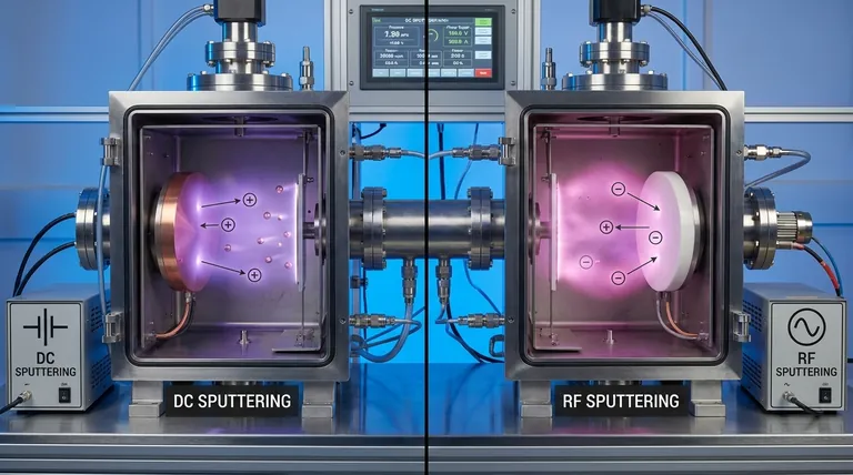
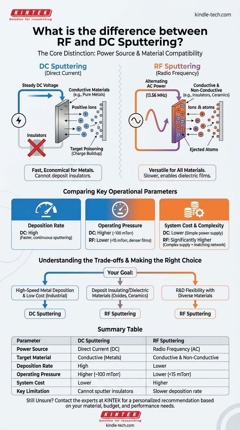
The fundamental difference between RF and DC sputtering lies in the type of power source they use and, consequently, the types of materials they can deposit. DC (Direct Current) sputtering uses a steady DC voltage and is highly effective for conductive materials like pure metals. RF (Radio Frequency) sputtering uses an alternating AC power source, which allows it to successfully deposit non-conductive, or insulating, materials—a task that is impossible for DC sputtering.
Your choice between these two methods is not arbitrary; it is dictated entirely by your target material. DC sputtering is the fast, economical workhorse for depositing metals, while RF sputtering provides the critical versatility needed for insulating (dielectric) thin films.
The Core Distinction: Power and Material Compatibility
The choice between RF and DC sputtering begins and ends with the electrical properties of the material you intend to deposit onto your substrate.
How DC Sputtering Works
In a DC sputtering system, a high DC voltage is applied to the target material, giving it a strong negative charge. This attracts positively charged ions from the plasma gas (like Argon).
These ions accelerate and strike the target with great force, knocking off atoms that then travel and deposit as a thin film on the substrate. This process is simple, fast, and highly efficient.
The Critical Limitation of DC
The DC method relies on the target material being electrically conductive to carry away the charge of the incoming positive ions.
If you attempt to use a non-conductive (insulating) material, such as a ceramic oxide, the positive charge from the ions rapidly accumulates on the target's surface. This buildup, known as "target poisoning," eventually repels any more incoming positive ions, halting the sputtering process and potentially causing damaging electrical arcs.
How RF Sputtering Solves the Problem
RF sputtering overcomes this limitation by using an AC power source that alternates its polarity at a radio frequency (typically 13.56 MHz).
In one half of the cycle, the target is negative, attracting ions and causing sputtering just like in a DC system. In the other half, the target becomes positive, attracting electrons from the plasma. These electrons instantly neutralize the positive charge that built up during the sputtering phase.
This rapid switching prevents charge accumulation, allowing for the continuous and stable sputtering of insulating materials.
Comparing Key Operational Parameters
Beyond material compatibility, the two methods differ in speed, operating conditions, and cost.
Deposition Rate and Efficiency
DC sputtering generally has a much higher deposition rate. Because its power is continuously dedicated to sputtering the target, it is significantly faster and more efficient for depositing metals.
RF sputtering is inherently slower because a portion of its cycle is used for charge neutralization rather than sputtering.
Operating Pressure
RF systems can sustain a stable plasma at lower gas pressures (e.g., under 15 mTorr) compared to DC systems (which may require up to 100 mTorr).
Lower pressure is often advantageous. It means there are fewer gas atoms between the target and the substrate, resulting in fewer collisions and a more direct path for sputtered atoms. This can lead to denser, higher-quality films.
System Complexity and Cost
A DC sputtering system is relatively simple and inexpensive, requiring only a high-voltage DC power supply.
An RF system is more complex and significantly more expensive. It requires a specialized RF power supply and an impedance-matching network to efficiently deliver power to the plasma, adding to both the initial cost and operational complexity.
Understanding the Trade-offs
Choosing a sputtering technique requires balancing your material needs against performance and budget constraints.
The Versatility vs. Speed Dilemma
RF sputtering offers unparalleled versatility, capable of depositing nearly any material, from pure metals to complex ceramic insulators. The trade-off for this flexibility is a lower deposition rate.
DC sputtering is a specialist. It does one thing—deposit conductive materials—extremely well, prioritizing speed and throughput above all else.
The Cost vs. Capability Dilemma
DC sputtering is the clear economic choice for high-volume production of metallic coatings. Its simplicity and efficiency keep operational costs down.
RF sputtering represents a necessary investment for research or manufacturing involving dielectric materials. The higher cost provides access to a class of materials that DC systems simply cannot handle.
Making the Right Choice for Your Goal
Your application's requirements will point directly to the correct technology.
- If your primary focus is depositing conductive metals at high speed and low cost: DC sputtering is the clear and superior choice, especially for industrial-scale applications.
- If your primary focus is depositing insulating (dielectric) materials like oxides, nitrides, or ceramics: RF sputtering is the essential and only viable option, as DC sputtering cannot process these materials.
- If your primary focus is research and development with diverse materials: An RF sputtering system provides the maximum flexibility, allowing you to experiment with both conductive and non-conductive targets.
Ultimately, understanding this core difference in power delivery empowers you to select the precise tool required for your material deposition goals.
Summary Table:
| Parameter | DC Sputtering | RF Sputtering |
|---|---|---|
| Power Source | Direct Current (DC) | Radio Frequency (AC) |
| Target Material | Conductive (Metals) | Conductive & Non-Conductive (Insulators, Ceramics) |
| Deposition Rate | High | Lower |
| Operating Pressure | Higher (~100 mTorr) | Lower (<15 mTorr) |
| System Cost | Lower | Higher |
| Key Limitation | Cannot sputter insulating materials | Slower deposition rate |
Still Unsure Which Sputtering Method is Right for Your Project?
Choosing between RF and DC sputtering is critical for achieving high-quality thin films. The experts at KINTEK can help you navigate this decision based on your specific material, budget, and performance requirements.
We specialize in providing precise lab equipment and consumables for all your deposition needs. Whether you're focused on high-throughput metal coatings with DC or versatile dielectric films with RF, we have the solution.
Contact our technical team today to discuss your application and get a personalized recommendation. Let KINTEK be your partner in advanced materials research and production.
#ContactForm to get started!
Visual Guide
Related Products
- Spark Plasma Sintering Furnace SPS Furnace
- Vacuum Induction Melting Spinning System Arc Melting Furnace
- Chemical Vapor Deposition CVD Equipment System Chamber Slide PECVD Tube Furnace with Liquid Gasifier PECVD Machine
- Customer Made Versatile CVD Tube Furnace Chemical Vapor Deposition Chamber System Equipment
People Also Ask
- Why are Spark Plasma Sintering (SPS) furnaces or hot presses utilized in the preparation of Li3PS4 solid electrolytes?
- What is the theory of spark plasma sintering? A Guide to Rapid, Low-Temperature Densification
- What is SPS sintering method? A Guide to High-Speed, High-Performance Material Fabrication
- What is the difference between spark plasma sintering and flash sintering? A Guide to Advanced Sintering Methods
- What is the process fundamentals of spark plasma sintering? Achieve Rapid, High-Density Material Consolidation


