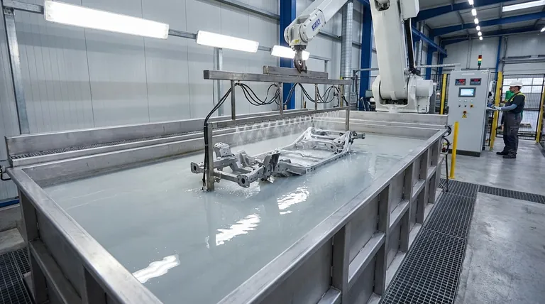
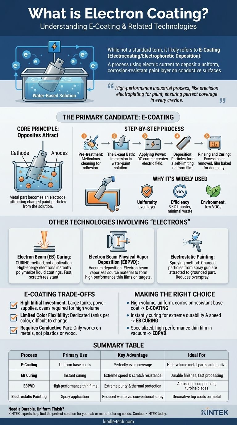
While "electron coating" is not a standard industry term, it almost certainly refers to E-coating, also known as electrocoating or electrophoretic deposition. This is a finishing process where an electric current is used to deposit a paint-like coating onto a conductive surface from a water-based solution, creating an exceptionally uniform and corrosion-resistant layer.
The term you've encountered likely means E-coating, a high-performance industrial process that functions like precision electroplating for paint. It uses an electrical charge to ensure every corner and crevice of a metal part receives a perfectly even protective film.

The Primary Candidate: Understanding E-Coating
E-coating is a cornerstone of modern manufacturing, especially in the automotive industry, for its ability to apply a robust base coat with unmatched consistency. It's best understood as an immersion process.
The Core Principle
At its heart, E-coating uses the principle of "opposites attract." The metal part to be coated is submerged in a bath containing charged paint particles suspended in water. An electric voltage is applied, turning the part into an electrode.
This electric field causes the charged paint particles to migrate through the liquid and deposit themselves onto the surface of the part.
The Step-by-Step Process
- Pre-treatment: The part must be meticulously cleaned to remove any oils, rust, or contaminants. This multi-stage chemical process is critical for ensuring proper adhesion.
- The E-coat Bath: The part is then immersed in the electrophoretic paint bath, which is typically around 80-90% deionized water and 10-20% paint solids.
- Applying Power: A direct current (DC) is applied. Depending on the type of E-coat, the part can be the anode (anodic) or, more commonly, the cathode (cathodic), which offers superior corrosion resistance.
- Deposition: The charged paint particles are drawn to the part, forming a smooth, continuous film. This film begins to insulate the part, so as an area gets coated, the electrical resistance increases, driving the particles to seek out uncoated bare metal. This "self-limiting" action is what guarantees a perfectly uniform thickness, even inside complex shapes and cavities.
- Rinsing and Curing: The part is removed from the bath and rinsed to remove any excess paint. It is then baked in an oven, which cures the film into a hard, durable, and smooth finish.
Why It's Widely Used
The primary advantages of E-coating are its uniformity and efficiency. Because the process coats any conductive surface it can reach, it provides comprehensive corrosion protection. Furthermore, the transfer efficiency is extremely high—often over 95%—resulting in minimal waste and making it an environmentally responsible choice with low VOCs (Volatile Organic Compounds).
Other Technologies Involving "Electrons"
The term "electron coating" might also be a conflation with other advanced finishing processes where electrons play a central role.
Electron Beam (EB) Curing
This is not an application method but a curing method. After a special coating is applied, it is bombarded with a high-energy beam of electrons. This beam provides the energy to instantly polymerize (cure) the coating, turning it from a liquid to a solid without heat. It's known for its incredible speed and producing extremely scratch-resistant surfaces.
Electron Beam Physical Vapor Deposition (EBPVD)
This is a highly specialized vacuum deposition technique. Inside a vacuum chamber, an electron beam is fired at a source material, such as a block of ceramic or metal, vaporizing it. This vapor then travels and condenses onto a target object (like a jet engine turbine blade), forming an extremely pure and high-performance thin film, often for thermal protection.
Electrostatic Painting
This is a common spraying method, often confused with E-coating. Here, liquid or powder coating particles are given an electrostatic charge as they leave the spray gun. The part to be coated is grounded. This creates an electrical attraction that pulls the coating particles to the part, reducing overspray and waste compared to conventional spraying.
Understanding the Trade-offs of E-Coating
While powerful, E-coating is not the right solution for every situation. Its primary limitations are rooted in the nature of the process.
High Initial Investment
The E-coating process requires large immersion tanks, sophisticated power supplies, pre-treatment stations, and curing ovens. This represents a significant capital investment best suited for high-volume production.
Limited Color Flexibility
An entire E-coat tank is dedicated to a single color. Changing colors is a massive, time-consuming, and expensive undertaking. For this reason, E-coating is most often used to apply primers in neutral colors like black or grey, which are then covered by a decorative top coat.
Requires a Conductive Part
The process relies entirely on electricity to work. Therefore, it can only be used on conductive materials, such as metals. Plastics, wood, or other non-conductive materials cannot be E-coated without special, and often impractical, preparatory steps.
Making the Right Choice for Your Goal
To ensure you are referencing the correct technology, consider your end goal.
- If your primary focus is a high-volume, uniform, and corrosion-resistant base coat for metal parts: You are almost certainly talking about E-coating (electrocoating).
- If your primary focus is instantly curing a finish for extreme durability and speed: You are likely thinking of Electron Beam (EB) Curing.
- If your primary focus is applying a specialized, high-performance thin film in a vacuum: The process you are looking for is Electron Beam Physical Vapor Deposition (EBPVD).
By distinguishing between these processes, you can accurately identify the technology needed to achieve a durable, high-quality finish for your specific application.
Summary Table:
| Process | Primary Use | Key Advantage | Ideal For |
|---|---|---|---|
| E-Coating (Electrocoating) | Applying uniform base coats | Perfectly even coverage, even in complex shapes | High-volume metal parts, automotive primers |
| Electron Beam (EB) Curing | Instant curing of coatings | Extreme speed and scratch resistance | Durable finishes requiring fast processing |
| Electron Beam PVD (EBPVD) | Depositing high-performance thin films | Extreme purity and thermal protection | Aerospace components, turbine blades |
| Electrostatic Painting | Spray application with reduced waste | Improved transfer efficiency over conventional spray | Decorative top coats on metal products |
Need a Durable, Uniform Finish for Your Metal Components?
Choosing the right coating process is critical for performance and longevity. The experts at KINTEK can help you navigate these advanced technologies to find the perfect solution for your laboratory or manufacturing needs.
We specialize in supplying high-quality lab equipment and consumables to support your finishing and coating applications. Whether you're exploring E-coating for corrosion resistance or need equipment for advanced deposition techniques, our team is here to provide the right tools and expertise.
Contact KINTEK today to discuss how we can help you achieve superior coating results with the right equipment and support.
Visual Guide
