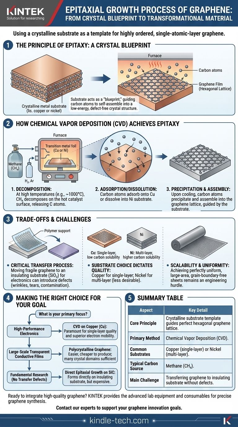
In essence, the epitaxial growth of graphene is a process where a crystalline substrate is used as a template to grow a highly ordered, single-atomic-layer sheet of carbon. Instead of carbon atoms randomly clumping together, they arrange themselves by mimicking the underlying crystal structure of the substrate, resulting in a large, high-quality graphene film with minimal defects. The most common industrial method for this is Chemical Vapor Deposition (CVD).
The core principle is simple: you are not just making graphene, you are templating it. Epitaxial growth uses a foundational crystal lattice to guide carbon atoms into forming the perfect hexagonal structure, unlocking the material's extraordinary electronic and mechanical properties.
The Principle of Epitaxy: A Crystal Blueprint
Epitaxy is a concept borrowed from crystal growth, where one crystal layer is grown on top of another.
The Substrate as a Template
Think of the substrate, typically a transition metal foil, as a perfectly laid-out blueprint. Its own atomic crystal structure provides a low-energy landscape for carbon atoms to settle into.
The carbon atoms, when deposited on this heated substrate, will naturally align with this blueprint, self-assembling into the honeycomb lattice of graphene. This templating effect is what separates epitaxial growth from other, less controlled synthesis methods.
How Chemical Vapor Deposition (CVD) Achieves Epitaxy
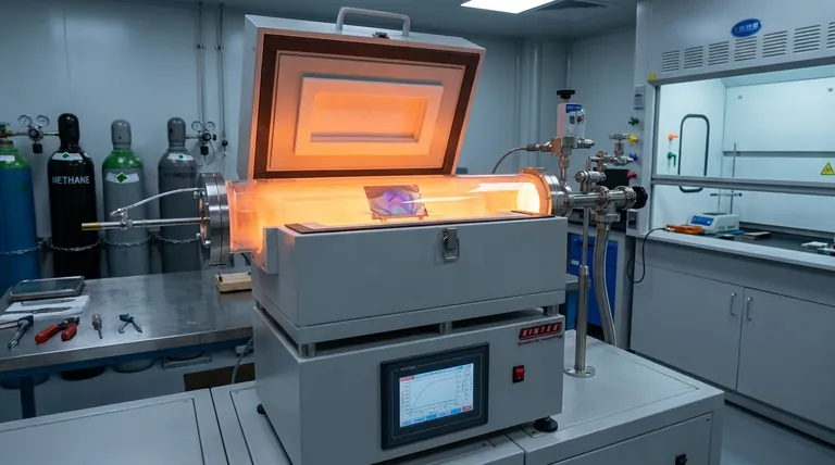
Chemical Vapor Deposition (CVD) is the most widely used technique for the epitaxial growth of large-area graphene. The process relies on a precise interplay of a catalyst, a carbon source, and specific atmospheric conditions.
The Role of the Substrate (Catalyst)
Transition metals like copper (Cu) or nickel (Ni) are used as the substrate. They serve two critical functions: they provide the crystalline template and they act as a catalyst.
At high temperatures inside a furnace, the metal surface actively breaks down the carbon-source gas, making individual carbon atoms available for growth. As noted, these metals are favored for their catalytic efficiency and relative cost-effectiveness.
The Carbon Source and Atmosphere
A carbon-containing precursor gas, most commonly methane (CH₄), is introduced into the furnace.
The reaction takes place in a controlled atmosphere, often with hydrogen (H₂) and argon (Ar) gases, which helps control the reaction rate and remove impurities.
The Growth Mechanism
The process typically involves three key steps:
- Decomposition: At high temperatures (~1000°C), the methane gas decomposes on the hot metal surface, releasing carbon atoms.
- Adsorption/Dissolution: Carbon atoms adsorb (on copper) or dissolve (into nickel) onto the metal substrate.
- Precipitation and Assembly: As the substrate is cooled, the carbon atoms' solubility decreases, and they precipitate back onto the surface. Guided by the metal's crystal lattice, they assemble into the hexagonal graphene structure.
Understanding the Trade-offs and Challenges
While epitaxial growth via CVD is powerful, it is not without its complexities and limitations. Understanding these trade-offs is crucial for practical applications.
The Critical Transfer Process
The biggest challenge is that graphene is grown on a metal conductor, but most electronic applications require it on an insulating substrate like silicon dioxide (SiO₂).
This requires a delicate transfer process, where the metal is etched away and the fragile graphene film is moved. This step can easily introduce wrinkles, tears, and contamination, negating the high quality achieved during growth.
Substrate Choice Dictates Quality
The choice of metal catalyst has a significant impact. Copper is preferred for growing single-layer graphene because of its very low carbon solubility.
Nickel, with higher carbon solubility, often leads to the growth of multi-layer graphene, which is not always desirable. This creates a direct trade-off between the material you want and the process you must use.
Scalability and Uniformity
Achieving a perfectly uniform, large-area, single-crystal graphene sheet without any grain boundaries remains a significant engineering hurdle. Scaling this process to industrial levels while maintaining flawless quality is the primary barrier to widespread adoption in high-end electronics.
Making the Right Choice for Your Goal
The ideal approach to graphene synthesis depends entirely on the intended application.
- If your primary focus is high-performance electronics: CVD growth on copper is the standard, as achieving a pristine single layer is paramount for superior electron mobility.
- If your primary focus is large-scale transparent conductive films: Polycrystalline graphene (with many small crystal domains) is often sufficient and is easier and cheaper to produce on a large scale.
- If your primary focus is fundamental research without transfer defects: Direct epitaxial growth on silicon carbide (SiC) is an option, as it forms graphene directly on an insulating substrate, but it is substantially more expensive.
Ultimately, mastering epitaxial growth is the key to moving graphene from a laboratory wonder to a transformative industrial material.
Summary Table:
| Aspect | Key Detail |
|---|---|
| Core Principle | Using a crystalline substrate as a template to guide carbon atoms into forming a perfect hexagonal graphene lattice. |
| Primary Method | Chemical Vapor Deposition (CVD). |
| Common Substrates | Copper (for single-layer) or Nickel (for multi-layer). |
| Typical Carbon Source | Methane (CH₄). |
| Main Challenge | Transferring the graphene from the metal growth substrate to an insulating substrate for electronic applications without introducing defects. |
| Ideal For | High-performance electronics (single-layer on Cu) or large-scale conductive films (polycrystalline). |
Ready to integrate high-quality graphene into your research or product development? The epitaxial growth process is complex, but the results are transformative. KINTEK specializes in providing the advanced lab equipment and consumables necessary for cutting-edge materials science like graphene synthesis. Our expertise can help you achieve the precise control needed for your specific application, whether it's for electronics, composites, or fundamental research.
Contact our experts today to discuss how we can support your laboratory's graphene innovation goals.
Visual Guide
Related Products
- Microwave Plasma Chemical Vapor Deposition MPCVD Machine System Reactor for Lab and Diamond Growth
- 915MHz MPCVD Diamond Machine Microwave Plasma Chemical Vapor Deposition System Reactor
- Cylindrical Resonator MPCVD Machine System Reactor for Microwave Plasma Chemical Vapor Deposition and Lab Diamond Growth
- HFCVD Machine System Equipment for Drawing Die Nano-Diamond Coating
- Chemical Vapor Deposition CVD Equipment System Chamber Slide PECVD Tube Furnace with Liquid Gasifier PECVD Machine
People Also Ask
- How does a microwave plasma reactor facilitate the synthesis of diamond? Master MPCVD with Precision Technology
- How are CVD diamonds created? Discover the Science of Lab-Grown Diamond Precision
- Why is argon-rich gas phase chemistry used for UNCD growth? Unlock Precision Nano-Diamond Synthesis
- How does MPCVD work? A Guide to Low-Temperature, High-Quality Film Deposition
- Why is MW-CVD preferred for high-purity diamond optical windows? Achieve Zero-Contamination Material Growth


