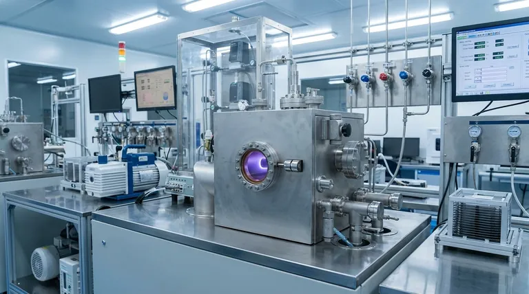
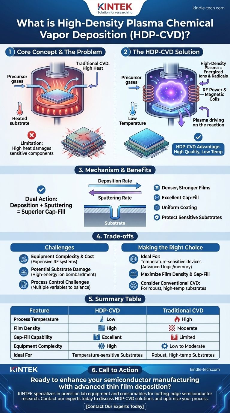
At its core, High-Density Plasma Chemical Vapor Deposition (HDP-CVD) is an advanced manufacturing process used to deposit exceptionally high-quality thin films onto a surface. Unlike traditional methods that rely solely on high heat, HDP-CVD uses an energized, high-density plasma to drive the chemical reactions needed to form the film, enabling the process to run at much lower temperatures.
HDP-CVD solves a critical manufacturing challenge: how to deposit a dense, uniform, and high-quality coating without using the high temperatures that would damage sensitive underlying components, particularly in advanced semiconductor fabrication.
The Foundation: Understanding Chemical Vapor Deposition (CVD)
What is Standard CVD?
Chemical Vapor Deposition is a process where a component, or substrate, is placed inside a vacuum chamber.
Volatile precursor chemicals are introduced into the chamber in gaseous form. These gases flow over the substrate.
Traditionally, the substrate is heated to a very high temperature. This thermal energy causes the precursor gases to react or decompose, depositing a solid thin film of the desired material onto the substrate's surface.
The Limitation of Heat
This reliance on high heat is the primary limitation of conventional CVD.
Many modern devices, such as integrated circuits with billions of tiny transistors, are built in layers. The components in the lower layers are often highly sensitive to temperature.
Exposing them to the heat required for traditional CVD could destroy or degrade them, making the entire device fail.
Introducing Plasma: The HDP-CVD Advantage
The Role of Plasma
Plasma-enhanced CVD (PECVD) introduces a new source of energy into the process. By applying an electric field, the precursor gas is ionized, creating a state of matter called plasma.
This plasma is a highly energetic soup of ions, electrons, and reactive radicals. These energized particles can drive the necessary chemical reactions for deposition without requiring extreme heat.
Why "High-Density" Matters
HDP-CVD takes this a step further. It uses specialized techniques to generate a plasma that is significantly denser—meaning it contains a much higher concentration of reactive ions and radicals—than in standard PECVD.
This high density of reactive species simultaneously increases the deposition rate (how fast the film grows) and the sputtering rate (an ion-driven cleaning effect). This dual action fills microscopic gaps more effectively and produces films that are denser, stronger, and more uniform.
The Key Benefit: Low-Temperature, High-Quality Films
The primary advantage of HDP-CVD is its ability to produce superior films at significantly lower process temperatures.
This makes it indispensable for applications where the substrate cannot tolerate high heat, which is the standard situation in modern microelectronics manufacturing.
Understanding the Trade-offs
Equipment Complexity and Cost
Generating and sustaining a high-density plasma requires complex and expensive hardware, including radio-frequency (RF) power generators and magnetic coils. This makes HDP-CVD systems more costly than conventional thermal CVD reactors.
Potential for Substrate Damage
While plasma enables low-temperature processing, the high-energy ions can also physically bombard the substrate. If not precisely controlled, this bombardment can cause damage to the sensitive device layers you are trying to protect.
Process Control Challenges
HDP-CVD is a more complex process with more variables to manage than thermal CVD. Engineers must carefully balance gas flow, pressure, RF power, and substrate temperature to achieve the desired film properties without causing damage, requiring significant process expertise.
Making the Right Choice for Your Goal
HDP-CVD is a specialized tool designed for specific, demanding applications.
- If your primary focus is depositing films on temperature-sensitive devices: HDP-CVD is often the only viable choice for creating high-quality dielectric layers in advanced logic and memory chips.
- If your primary focus is achieving maximum film density and gap-fill: The unique deposition-sputtering mechanism of HDP-CVD provides superior results for filling deep, narrow trenches without creating voids.
- If your primary focus is low-cost deposition on a robust substrate: A simpler, less expensive method like conventional thermal CVD may be more appropriate if the substrate can withstand high temperatures.
Ultimately, HDP-CVD provides a powerful solution for manufacturing advanced materials where both film quality and low process temperatures are non-negotiable.
Summary Table:
| Feature | HDP-CVD | Traditional CVD |
|---|---|---|
| Process Temperature | Low | High |
| Film Density | High | Moderate |
| Gap-Fill Capability | Excellent | Limited |
| Equipment Complexity | High | Low to Moderate |
| Ideal For | Temperature-sensitive substrates | Robust, high-temperature substrates |
Ready to enhance your semiconductor manufacturing with advanced thin film deposition?
KINTEK specializes in precision lab equipment and consumables for cutting-edge semiconductor and materials research. Our expertise in plasma-enhanced deposition technologies can help you achieve superior film quality while protecting temperature-sensitive components.
Contact our experts today to discuss how HDP-CVD solutions can optimize your manufacturing process and deliver the high-density, uniform films your research demands.
Visual Guide
Related Products
- HFCVD Machine System Equipment for Drawing Die Nano-Diamond Coating
- Multi Heating Zones CVD Tube Furnace Machine Chemical Vapor Deposition Chamber System Equipment
- Split Chamber CVD Tube Furnace with Vacuum Station Chemical Vapor Deposition System Equipment Machine
- Chemical Vapor Deposition CVD Equipment System Chamber Slide PECVD Tube Furnace with Liquid Gasifier PECVD Machine
- Customer Made Versatile CVD Tube Furnace Chemical Vapor Deposition Chamber System Equipment
People Also Ask
- Why is Chemical Vapor Deposition (CVD) equipment uniquely suited for constructing hierarchical superhydrophobic structures?
- What is the chemical vapor deposition growth process? Build Superior Thin Films from the Atom Up
- What is the full form of HFCVD? A Guide to Hot Filament Chemical Vapor Deposition
- What types of substrates are used in CVD to facilitate graphene films? Optimize Graphene Growth with the Right Catalyst
- How expensive is chemical vapor deposition? Understanding the True Cost of High-Performance Coating


