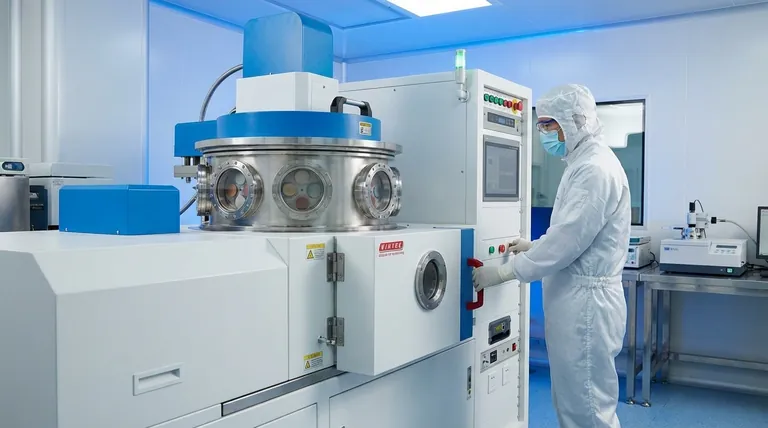
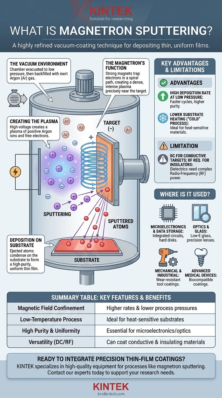
At its core, magnetron sputtering is a highly refined vacuum-coating technique used to deposit exceptionally thin, uniform films of material onto a surface. It operates by creating a plasma and using a magnetic field to confine it near a source material, or "target." This concentrated plasma bombards the target, ejecting atoms that then travel and condense onto a substrate, forming the desired coating layer by layer.
The essential innovation of magnetron sputtering is its use of a magnetic field. This field traps electrons near the target, dramatically increasing the efficiency of the plasma, which allows for faster, more controlled deposition at lower temperatures and pressures than other methods.
How Magnetron Sputtering Works: A Step-by-Step Breakdown
To understand why this method is so widely used, it's best to break it down into its core operational steps. The entire process takes place inside a sealed vacuum chamber.
The Vacuum Environment: Setting the Stage
First, the chamber is evacuated to a very low pressure. It is then backfilled with a small, controlled amount of an inert gas, most commonly Argon (Ar). This pristine, low-pressure environment ensures the sputtered atoms can travel from the target to the substrate without colliding with unwanted air molecules.
Creating the Plasma: The Role of Electrical Energy
A high-voltage power supply is applied between two electrodes. The material to be deposited, known as the target, is made into the negative electrode (cathode).
This strong electric field energizes the chamber, stripping electrons from the argon gas atoms. This process, called ionization, creates a glowing mixture of positive argon ions and free electrons known as a plasma.
The Magnetron's Critical Function: Concentrating the Bombardment
This is the key step that defines the process. A set of strong permanent magnets, the magnetron, is placed behind the target.
This magnetic field traps the free electrons, forcing them into a spiral path directly in front of the target's surface. This electron trap dramatically increases the probability of collision with argon gas atoms, creating a much denser, more intense plasma precisely where it is needed most.
Sputtering and Deposition: From Target to Substrate
The positively charged argon ions in this dense plasma are accelerated by the electric field and slam into the negatively charged target with great force.
Each impact has enough energy to knock out, or "sputter," one or more atoms from the target material. These ejected atoms are neutral and are not affected by the magnetic or electric fields. They travel in a straight line until they strike the substrate (the part being coated), where they condense to form a high-purity, uniform thin film.
Understanding the Trade-offs and Advantages
Magnetron sputtering is not used by accident; its specific characteristics offer significant advantages but also present certain limitations.
Key Advantage: High Deposition Rate at Low Pressure
The magnetron's efficiency in generating plasma means the process can run at much higher deposition speeds and lower gas pressures compared to simple sputtering. This translates to faster production cycles and higher-purity films.
Key Advantage: Lower Substrate Heating
Because the plasma is confined so effectively near the target, less stray energy bombards the substrate. This makes magnetron sputtering a "non-thermal" or "cold" process, ideal for coating heat-sensitive materials like plastics, polymers, and complex electronic devices without causing damage.
The Limitation of DC vs. RF Sputtering
The most common form, DC magnetron sputtering, uses a direct current power supply. This works exceptionally well for electrically conductive targets like metals.
However, if the target material is an electrical insulator (a dielectric, like a ceramic), a positive charge will build up on its surface, repelling the positive argon ions and quickly extinguishing the sputtering process. For these materials, a more complex method using a radio-frequency (RF) power supply is required.
Where is Magnetron Sputtering Used?
The precision, purity, and versatility of magnetron sputtering have made it a cornerstone technology across numerous advanced industries.
In Microelectronics and Data Storage
The semiconductor industry relies heavily on this method for depositing the thin metallic layers that form the wiring in integrated circuits. It was also a foundational technology in manufacturing computer hard disks.
In Optics and Glass
High-performance optical coatings for lenses, mirrors, and filters are often applied with magnetron sputtering. It is also the primary method for producing modern low-emissivity (Low-E) glass for energy-efficient windows, which have a transparent metallic coating that reflects thermal radiation.
In Mechanical and Industrial Applications
Extremely hard and wear-resistant coatings (like titanium nitride) are sputtered onto cutting tools, drills, and engine components to dramatically extend their lifespan. Self-lubricating films can also be applied to reduce friction in moving parts.
In Advanced Medical Devices
The ability to create pure, dense, and biocompatible coatings is critical in medicine. The process is used to coat dental and orthopedic implants, apply anti-rejection layers to devices, and manufacture components for angioplasty.
How to Apply This to Your Project
Your choice of a deposition technology depends entirely on the required properties of the final film.
- If your primary focus is high-performance electronics: Magnetron sputtering offers the precision and low-temperature deposition necessary for creating complex integrated circuits without damaging the underlying components.
- If your primary focus is advanced optical coatings: This method provides exceptional control over film thickness and uniformity, which is critical for manufacturing high-quality filters, mirrors, and functional glass.
- If your primary focus is durable mechanical surfaces: It is the industry standard for applying hard, wear-resistant, or low-friction films onto tools and industrial components for enhanced performance.
- If your primary focus is biocompatible medical implants: The process creates pure, dense coatings that improve the safety and performance of devices designed for use inside the human body.
Ultimately, magnetron sputtering provides an unparalleled level of atomic-scale control, making it an essential tool for modern high-technology manufacturing.
Summary Table:
| Key Feature | Benefit |
|---|---|
| Magnetic Field Confinement | Higher deposition rates & lower process pressures |
| Low-Temperature Process | Ideal for heat-sensitive substrates like plastics |
| High Purity & Uniformity | Essential for microelectronics and optical coatings |
| Versatility (DC/RF) | Can coat both conductive and insulating materials |
Ready to integrate precision thin-film coatings into your laboratory workflow? KINTEK specializes in providing high-quality lab equipment and consumables for advanced deposition processes like magnetron sputtering. Whether you are developing microelectronics, optical components, or medical devices, our solutions ensure the purity and uniformity your research demands. Contact our experts today to discuss how we can support your laboratory's specific needs.
Visual Guide
Related Products
- Spark Plasma Sintering Furnace SPS Furnace
- RF PECVD System Radio Frequency Plasma-Enhanced Chemical Vapor Deposition RF PECVD
People Also Ask
- What is SPS sintering method? A Guide to High-Speed, High-Performance Material Fabrication
- What is the process fundamentals of spark plasma sintering? Achieve Rapid, High-Density Material Consolidation
- What is the difference between spark plasma sintering and flash sintering? A Guide to Advanced Sintering Methods
- What are the fundamentals of spark plasma sintering process? Unlock Rapid, High-Performance Material Consolidation
- What is the theory of spark plasma sintering? A Guide to Rapid, Low-Temperature Densification

