Knowledge What is meant by uniformity of the film? The Key to Reliable Thin-Film Performance
Author avatar

Tech Team · Kintek Solution

Updated 4 days ago

What is meant by uniformity of the film? The Key to Reliable Thin-Film Performance


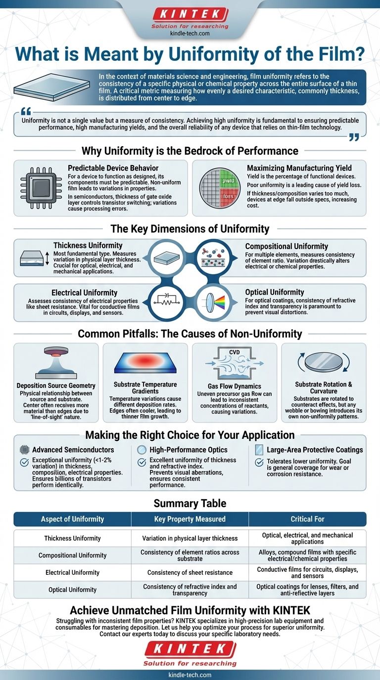
In the context of materials science and engineering, film uniformity refers to the consistency of a specific physical or chemical property across the entire surface of a thin film. It is a critical metric that measures how evenly a desired characteristic, most commonly thickness, is distributed from the center to the edge of a substrate.

Uniformity is not a single value but a measure of consistency. Achieving high uniformity is fundamental to ensuring predictable performance, high manufacturing yields, and the overall reliability of any device that relies on thin-film technology.

What is meant by uniformity of the film? The Key to Reliable Thin-Film Performance

Why Uniformity is the Bedrock of Performance

In nearly every application of thin films—from microchips to eyeglasses—inconsistency is a direct cause of failure or poor performance. Uniformity is the primary indicator of a well-controlled and repeatable manufacturing process.

Predictable Device Behavior

For a device to function as designed, its components must be predictable. A non-uniform film leads to variations in properties across a single device or from one device to another on the same wafer.

In semiconductors, for example, the thickness of a gate oxide layer directly controls the transistor's switching characteristics. If this film is not uniform, transistors across the chip will behave differently, leading to processing errors.

Maximizing Manufacturing Yield

Yield is the percentage of functional devices produced from a single manufacturing run (e.g., on a silicon wafer). Poor film uniformity is a leading cause of yield loss.

If a film's thickness or composition varies too much, devices at the edge of the wafer may fall outside of acceptable performance specifications, rendering them useless and driving up the cost per functional chip.

The Key Dimensions of Uniformity

While thickness is the most commonly discussed metric, uniformity applies to any critical film property that can be measured and mapped across a surface.

Thickness Uniformity

This is the most fundamental type. It measures the variation in the physical thickness of the deposited layer. It is crucial for optical, electrical, and mechanical applications.

Compositional Uniformity

For films made of multiple elements (alloys or compounds), this measures how consistent the ratio of those elements is across the substrate. A variation in composition can drastically alter a film's electrical or chemical properties.

Electrical Uniformity

This assesses the consistency of electrical properties, such as sheet resistance. It is vital for conductive films used in integrated circuits, transparent conductors for displays, and sensor electrodes.

Optical Uniformity

For optical coatings, the uniformity of properties like refractive index and transparency is paramount. Inconsistent optical properties on a lens, for example, would result in visible distortions or color variations.

Common Pitfalls: The Causes of Non-Uniformity

Achieving high uniformity requires precise control over the film deposition process. Non-uniformity is not random; it is typically a systematic outcome of the deposition environment.

Deposition Source Geometry

The physical relationship between the material source (e.g., a sputtering target) and the substrate is critical. The "line-of-sight" nature of many deposition techniques means the center of the substrate often receives more material than the edges.

Substrate Temperature Gradients

Temperature variations across the substrate can cause different reaction or deposition rates. The edges of a substrate holder are often cooler than the center, leading to thinner film growth in those areas.

Gas Flow Dynamics

In chemical vapor deposition (CVD), the flow of precursor gases must be carefully managed. Turbulent or uneven flow can lead to inconsistent concentrations of reactants across the surface, causing variations in film growth.

Substrate Rotation and Curvature

To counteract these effects, substrates are almost always rotated during deposition. However, any wobble in the rotation or curvature (bowing) of the substrate itself can introduce its own patterns of non-uniformity.

Making the Right Choice for Your Application

The required level of uniformity is dictated entirely by the end-use application. Understanding your primary goal is key to setting the right process specifications.

  • If your primary focus is advanced semiconductors: You require exceptional uniformity (often <1-2% variation) in thickness, composition, and electrical properties to ensure billions of transistors perform identically.
  • If your primary focus is high-performance optics: You need excellent uniformity of thickness and refractive index to prevent visual aberrations and ensure consistent anti-reflective or filtering performance.
  • If your primary focus is large-area protective coatings: You can often tolerate lower uniformity, as the goal is general coverage for wear or corrosion resistance rather than micro-scale device performance.

Ultimately, controlling film uniformity is about mastering the deposition process to deliver consistent, reliable performance where it matters most.

Summary Table:

Aspect of Uniformity Key Property Measured Critical For
Thickness Uniformity Variation in physical layer thickness Optical, electrical, and mechanical applications
Compositional Uniformity Consistency of element ratios across the substrate Alloys and compound films with specific electrical/chemical properties
Electrical Uniformity Consistency of sheet resistance and other electrical properties Conductive films for circuits, displays, and sensors
Optical Uniformity Consistency of refractive index and transparency Optical coatings for lenses, filters, and anti-reflective layers

Achieve Unmatched Film Uniformity with KINTEK

Struggling with inconsistent film properties that impact your device performance and manufacturing yield? KINTEK specializes in providing high-precision lab equipment and consumables designed to master the deposition process. Whether you are working on semiconductors, optical coatings, or protective layers, our solutions help you deliver the consistent, reliable results your application demands.

Let us help you optimize your process for superior uniformity. Contact our experts today to discuss your specific laboratory needs and discover how KINTEK can enhance your thin-film technology.

Visual Guide

What is meant by uniformity of the film? The Key to Reliable Thin-Film Performance Visual Guide

Related Products

People Also Ask

Related Products

RF PECVD System Radio Frequency Plasma-Enhanced Chemical Vapor Deposition RF PECVD

RF PECVD System Radio Frequency Plasma-Enhanced Chemical Vapor Deposition RF PECVD

RF-PECVD is an acronym for "Radio Frequency Plasma-Enhanced Chemical Vapor Deposition." It deposits DLC (Diamond-like carbon film) on germanium and silicon substrates. It is utilized in the 3-12um infrared wavelength range.

Inclined Rotary Plasma Enhanced Chemical Vapor Deposition PECVD Equipment Tube Furnace Machine

Inclined Rotary Plasma Enhanced Chemical Vapor Deposition PECVD Equipment Tube Furnace Machine

Upgrade your coating process with PECVD coating equipment. Ideal for LED, power semiconductors, MEMS and more. Deposits high-quality solid films at low temps.

Customer Made Versatile CVD Tube Furnace Chemical Vapor Deposition Chamber System Equipment

Customer Made Versatile CVD Tube Furnace Chemical Vapor Deposition Chamber System Equipment

Get your exclusive CVD furnace with KT-CTF16 Customer Made Versatile Furnace. Customizable sliding, rotating, and tilting functions for precise reactions. Order now!

Chemical Vapor Deposition CVD Equipment System Chamber Slide PECVD Tube Furnace with Liquid Gasifier PECVD Machine

Chemical Vapor Deposition CVD Equipment System Chamber Slide PECVD Tube Furnace with Liquid Gasifier PECVD Machine

KT-PE12 Slide PECVD System: Wide power range, programmable temp control, fast heating/cooling with sliding system, MFC mass flow control & vacuum pump.

915MHz MPCVD Diamond Machine Microwave Plasma Chemical Vapor Deposition System Reactor

915MHz MPCVD Diamond Machine Microwave Plasma Chemical Vapor Deposition System Reactor

915MHz MPCVD Diamond Machine and its multi-crystal effective growth, the maximum area can reach 8 inches, the maximum effective growth area of single crystal can reach 5 inches. This equipment is mainly used for the production of large-size polycrystalline diamond films, the growth of long single crystal diamonds, the low-temperature growth of high-quality graphene, and other materials that require energy provided by microwave plasma for growth.

HFCVD Machine System Equipment for Drawing Die Nano-Diamond Coating

HFCVD Machine System Equipment for Drawing Die Nano-Diamond Coating

The nano-diamond composite coating drawing die uses cemented carbide (WC-Co) as the substrate, and uses the chemical vapor phase method ( CVD method for short ) to coat the conventional diamond and nano-diamond composite coating on the surface of the inner hole of the mold.

Split Chamber CVD Tube Furnace with Vacuum Station Chemical Vapor Deposition System Equipment Machine

Split Chamber CVD Tube Furnace with Vacuum Station Chemical Vapor Deposition System Equipment Machine

Efficient split chamber CVD furnace with vacuum station for intuitive sample checking and quick cooling. Up to 1200℃ max temperature with accurate MFC mass flowmeter control.

Vacuum Hot Press Furnace Machine for Lamination and Heating

Vacuum Hot Press Furnace Machine for Lamination and Heating

Experience clean and precise lamination with Vacuum Lamination Press. Perfect for wafer bonding, thin-film transformations, and LCP lamination. Order now!

VHP Sterilization Equipment Hydrogen Peroxide H2O2 Space Sterilizer

VHP Sterilization Equipment Hydrogen Peroxide H2O2 Space Sterilizer

A hydrogen peroxide space sterilizer is a device that uses vaporized hydrogen peroxide to decontaminate enclosed spaces. It kills microorganisms by damaging their cellular components and genetic material.

Anti-Cracking Press Mold for Lab Use

Anti-Cracking Press Mold for Lab Use

The anti-cracking press mold is a specialized equipment designed for molding various shapes and sizes of film using high pressure and electric heating.

Laboratory Sterilizer Lab Autoclave Vertical Pressure Steam Sterilizer for Liquid Crystal Display Automatic Type

Laboratory Sterilizer Lab Autoclave Vertical Pressure Steam Sterilizer for Liquid Crystal Display Automatic Type

Liquid crystal display automatic vertical sterilizer is a safe, reliable and automatic control sterilization equipment, which is composed of heating system, microcomputer control system and overheating and overvoltage protection system.

1200℃ Split Tube Furnace with Quartz Tube Laboratory Tubular Furnace

1200℃ Split Tube Furnace with Quartz Tube Laboratory Tubular Furnace

KT-TF12 split tube furnace: high-purity insulation, embedded heating wire coils, and max. 1200C. Widely used for new materials and chemical vapour deposition.

Benchtop Laboratory Freeze Dryer for Lab Use

Benchtop Laboratory Freeze Dryer for Lab Use

Premium benchtop laboratory freeze dryer for lyophilization, preserving samples with ≤ -60°C cooling. Ideal for pharmaceuticals & research.

Laboratory Test Sieves and Sieving Machines

Laboratory Test Sieves and Sieving Machines

Precision lab test sieves & sieving machines for accurate particle analysis. Stainless steel, ISO-compliant, 20μm-125mm range. Request specs now!

High Performance Laboratory Freeze Dryer

High Performance Laboratory Freeze Dryer

Advanced lab freeze dryer for lyophilization, preserving biological & chemical samples efficiently. Ideal for biopharma, food, and research.

Rotating Platinum Disk Electrode for Electrochemical Applications

Rotating Platinum Disk Electrode for Electrochemical Applications

Upgrade your electrochemical experiments with our Platinum Disc Electrode. High-quality and reliable for accurate results.

Laboratory Vibratory Sieve Shaker Machine Slap Vibrating Sieve

Laboratory Vibratory Sieve Shaker Machine Slap Vibrating Sieve

KT-T200TAP is a slapping and oscillating sieving instrument for laboratory desktop use, with 300 rpm horizontal circular motion and 300 vertical slapping motions to simulate manual sieving to help sample particles pass through better.

Graphite Vacuum Continuous Graphitization Furnace

Graphite Vacuum Continuous Graphitization Furnace

High-temperature graphitization furnace is a professional equipment for graphitization treatment of carbon materials. It is a key equipment for the production of high-quality graphite products. It has high temperature, high efficiency and uniform heating. It is suitable for various high-temperature treatments and graphitization treatments. It is widely used in metallurgy, electronics, aerospace, etc. industry.

Small Vacuum Heat Treat and Tungsten Wire Sintering Furnace

Small Vacuum Heat Treat and Tungsten Wire Sintering Furnace

The small vacuum tungsten wire sintering furnace is a compact experimental vacuum furnace specially designed for universities and scientific research institutes. The furnace features a CNC welded shell and vacuum piping to ensure leak-free operation. Quick-connect electrical connections facilitate relocation and debugging, and the standard electrical control cabinet is safe and convenient to operate.

Non Consumable Vacuum Arc Induction Melting Furnace

Non Consumable Vacuum Arc Induction Melting Furnace

Explore the benefits of Non-Consumable Vacuum Arc Furnace with high melting point electrodes. Small, easy to operate & eco-friendly. Ideal for laboratory research on refractory metals & carbides.


Leave Your Message