In essence, Physical Vapor Deposition (PVD) for crystal growth is a family of vacuum-based techniques where a solid material is vaporized, travels atom by atom through a vacuum, and condenses onto a target surface (the substrate) to form a high-quality, crystalline thin film. Unlike simple coating, the goal here is not just to cover a surface but to precisely arrange the arriving atoms into an ordered, single-crystal structure.
While often discussed as a coating method, PVD's true power in crystal growth lies in its atomic-level control. By manipulating a material in its vapor phase within a vacuum, PVD enables the fabrication of high-purity, ultra-thin crystalline films that are often impossible to create with traditional melt-based techniques.
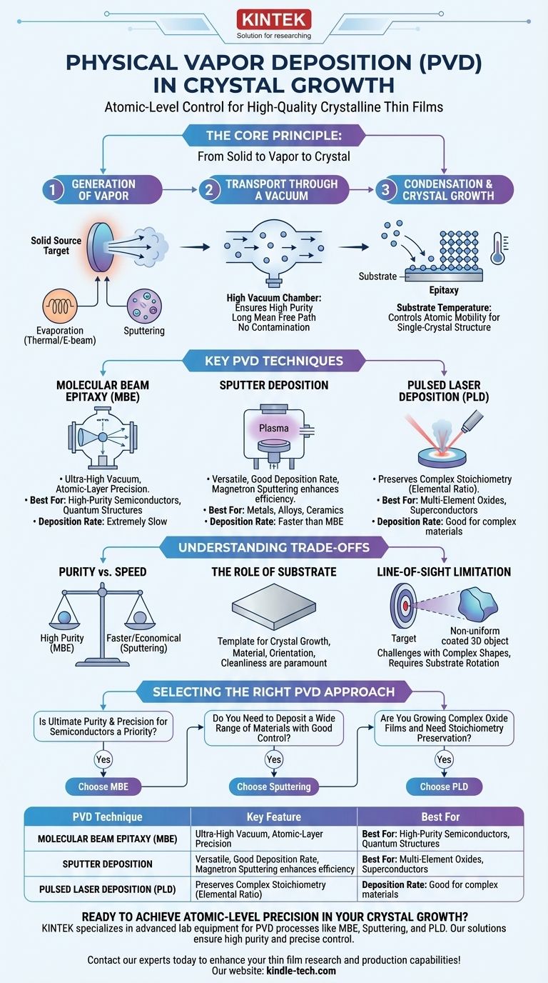
The Core Principle: From Solid to Vapor to Crystal
At its heart, every PVD process for crystal growth follows a three-step sequence. Understanding this sequence is key to understanding the entire field.
Step 1: Generation of Vapor
The first step is to convert a solid source material, known as the target, into a gaseous vapor. This is achieved primarily through two physical (not chemical) mechanisms.
- Evaporation: The target material is heated in a vacuum until its atoms or molecules gain enough thermal energy to escape the surface and become a vapor. This can be done by resistive heating (Thermal Evaporation) or by bombarding it with a high-energy electron beam (E-beam Evaporation).
- Sputtering: The target is placed in a low-pressure environment with an inert gas, typically Argon. A strong electric field ignites a plasma, and the resulting high-energy ions are accelerated into the target, physically knocking off or "sputtering" atoms from its surface.
Step 2: Transport Through a Vacuum
The vaporized atoms travel from the source target to the substrate. This journey takes place inside a high-vacuum chamber.
The vacuum is critical for two reasons. First, it ensures high purity by removing air, water, and other reactive molecules that could contaminate the growing crystal. Second, it creates a long mean free path, meaning the vaporized atoms can travel in a straight line to the substrate without colliding with other gas molecules.
Step 3: Condensation and Crystal Growth
When the vapor atoms arrive at the substrate, they condense back into a solid. For crystal growth to occur, these atoms must have enough mobility to move around on the surface and settle into the lowest-energy positions, forming an ordered lattice.
This process, known as epitaxy, is heavily influenced by the substrate temperature. A carefully controlled temperature provides the arriving atoms (or "adsorbates") with the thermal energy needed to arrange themselves into a single-crystal film that often mimics the crystal structure of the underlying substrate.
Key PVD Techniques for Crystal Growth
PVD is not one method but a category. The specific technique chosen depends entirely on the desired material, purity, and structural quality.
Molecular Beam Epitaxy (MBE)
MBE is the gold standard for creating the highest-purity single-crystal films, especially for advanced semiconductors. It uses thermal evaporation from ultra-pure elemental sources in an ultra-high vacuum (UHV) environment.
The deposition rates are extremely slow, allowing for true atomic layer-by-layer growth. This precision enables the fabrication of complex quantum wells and superlattices with atomically sharp interfaces.
Sputter Deposition
Sputtering is an incredibly versatile and widely used PVD technique for a broad range of materials, including metals, alloys, and ceramics.
While generally faster than MBE, the plasma environment can make it less "delicate." However, modern magnetron sputtering uses magnetic fields to confine the plasma near the target, increasing efficiency and minimizing substrate damage, making it suitable for high-quality crystalline film growth.
Pulsed Laser Deposition (PLD)
In PLD, a high-power pulsed laser is focused on the target inside a vacuum chamber. Each laser pulse ablates a small amount of material, creating a high-energy plasma plume that expands toward the substrate.
PLD is exceptionally good at depositing materials with complex chemical formulas (e.g., multi-element oxides) because the explosive ablation process tends to preserve the stoichiometry (the elemental ratio) of the target material in the final film.
Understanding the Trade-offs
Choosing a PVD method involves balancing competing factors. There is no single "best" technique; there is only the best technique for a specific goal.
Purity vs. Speed
MBE offers unparalleled purity due to the UHV environment, but it is extremely slow and expensive. Sputtering is much faster and more economical but carries a higher risk of incorporating the sputtering gas (e.g., Argon) as an impurity in the growing film.
The Critical Role of the Substrate
The substrate is not a passive component; it is the template for crystal growth. Its material, crystal orientation, and cleanliness are paramount. An improperly prepared substrate will result in a poor-quality, polycrystalline, or amorphous film, regardless of the PVD technique used.
Line-of-Sight Limitation
A fundamental characteristic of most PVD processes is that they are line-of-sight. The vapor travels in a straight line from the source to the substrate. This makes it challenging to uniformly coat complex, three-dimensional shapes without sophisticated substrate rotation mechanisms.
PVD vs. Chemical Vapor Deposition (CVD)
The primary alternative to PVD is Chemical Vapor Deposition (CVD). CVD uses chemical reactions of precursor gases on a heated substrate to form the film. While CVD can offer better coverage over complex shapes (it's not line-of-sight), PVD often provides higher purity and works with a wider range of materials that lack suitable gaseous precursors.
Selecting the Right PVD Approach for Your Goal
Your choice of PVD technique should be driven by the specific requirements of the crystal film you intend to grow.
- If your primary focus is ultimate purity and atomic-layer precision for semiconductors: Molecular Beam Epitaxy (MBE) is the definitive choice, despite its complexity and cost.
- If your primary focus is depositing a wide range of materials, including complex alloys or ceramics, with good control: Sputter Deposition offers the best balance of versatility, deposition rate, and scalability.
- If your primary focus is growing high-quality complex oxide films (e.g., for superconductors or ferroelectrics): Pulsed Laser Deposition (PLD) excels at preserving the stoichiometry of the source material in the final film.
Ultimately, mastering PVD is about understanding it not as a single method, but as a toolkit for precisely engineering crystalline materials at the atomic scale.
Summary Table:
| PVD Technique | Key Feature | Best For |
|---|---|---|
| Molecular Beam Epitaxy (MBE) | Ultra-high vacuum, atomic-layer precision | High-purity semiconductors, quantum structures |
| Sputter Deposition | Versatile, good deposition rate | Metals, alloys, ceramics |
| Pulsed Laser Deposition (PLD) | Preserves complex stoichiometry | Multi-element oxides, superconductors |
Ready to achieve atomic-level precision in your crystal growth? KINTEK specializes in providing advanced lab equipment and consumables tailored for PVD processes like MBE, sputtering, and PLD. Whether you're developing next-generation semiconductors or complex oxide films, our solutions ensure high purity and precise control. Contact our experts today to enhance your thin film research and production capabilities!
Visual Guide
Related Products
- Chemical Vapor Deposition CVD Equipment System Chamber Slide PECVD Tube Furnace with Liquid Gasifier PECVD Machine
- RF PECVD System Radio Frequency Plasma-Enhanced Chemical Vapor Deposition RF PECVD
- 915MHz MPCVD Diamond Machine Microwave Plasma Chemical Vapor Deposition System Reactor
- HFCVD Machine System Equipment for Drawing Die Nano-Diamond Coating
- Microwave Plasma Chemical Vapor Deposition MPCVD Machine System Reactor for Lab and Diamond Growth
People Also Ask
- What happens during deposition chemistry? Building Thin Films from Gaseous Precursors
- How are carbon nanotubes grown? Master Scalable Production with Chemical Vapor Deposition
- What are the advantages of chemical vapor deposition? Achieve Superior Thin Films for Your Lab
- What is the chemical vapor deposition growth process? Build Superior Thin Films from the Atom Up
- What are the processes of vapor phase deposition? Understand CVD vs. PVD for Superior Thin Films


