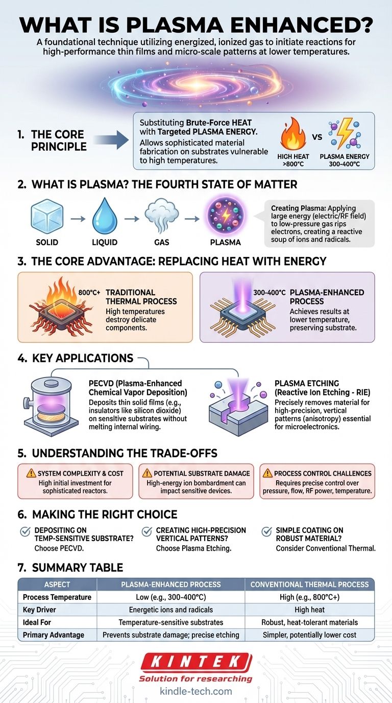
In the world of advanced manufacturing and materials science, the term “plasma enhanced” refers to a process that utilizes plasma—an energized, ionized gas—to initiate or dramatically accelerate a physical or chemical reaction. It is a foundational technique for creating the high-performance thin films and micro-scale patterns required for modern electronics, optics, and tools, often achieving results at much lower temperatures than conventional methods.
The core principle of any plasma-enhanced process is substituting the brute-force energy of high heat with the targeted chemical and physical energy of a plasma. This allows for sophisticated material fabrication on substrates that would otherwise be damaged or destroyed by traditional high-temperature techniques.
What is Plasma? The "Fourth State of Matter"
To understand why plasma is so useful, we first need to understand what it is. It's often called the fourth state of matter, alongside solid, liquid, and gas.
Creating the Plasma
You create a plasma by applying a large amount of energy—typically from a strong electric or radio-frequency (RF) field—to a gas at very low pressure.
This energy rips electrons from the gas atoms or molecules, creating a super-heated soup of free electrons, positively charged ions, and remaining neutral particles. This mix is the plasma, and it is highly reactive.
The Key to Reactivity
While the plasma as a whole can be very hot, the key is that the individual particles (especially the electrons) carry immense kinetic energy. These energetic particles collide with neutral gas molecules, breaking them apart into highly reactive species called radicals.
It is these radicals and ions, not just high temperature, that drive the desired chemical reactions.
The Core Advantage: Replacing Heat with Energy
The fundamental reason for using plasma-enhanced processes is to bypass the need for extreme heat, which is a major limitation in fabricating complex devices.
The Problem with High Temperatures
Many advanced manufacturing steps, like depositing a thin film of silicon nitride, traditionally require temperatures of 800°C or more.
If you are building a microchip, such high temperatures would destroy the delicate aluminum or copper wiring already fabricated on the silicon wafer. The device would be ruined.
How Plasma Solves the Problem
A plasma-enhanced process can achieve the same result at a much lower temperature, often around 300-400°C.
The energy from the plasma breaks down the precursor gases into the necessary reactive components. These components then react on the wafer's surface to form the desired film, without ever needing the damaging high temperatures.
Key Applications of Plasma Enhancement
Plasma-enhanced techniques are critical in semiconductor manufacturing and materials science. The two most common applications are deposition and etching.
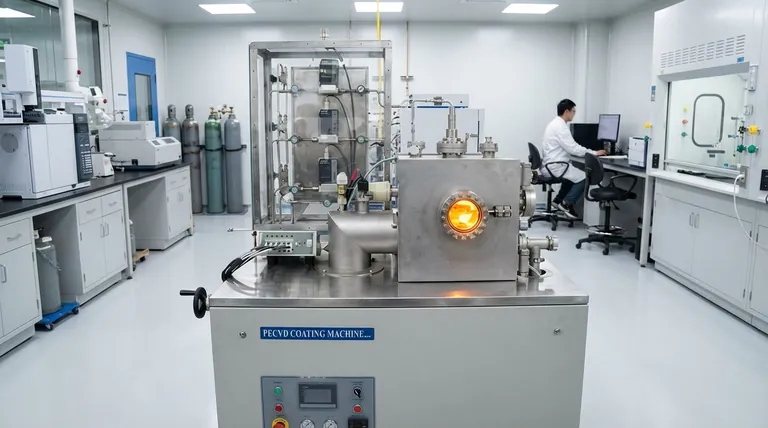
Plasma-Enhanced Chemical Vapor Deposition (PECVD)
PECVD is a process used to deposit thin solid films onto a substrate. Precursor gases are introduced into a vacuum chamber, the plasma is ignited, and the resulting radicals react at the substrate surface to build the film layer by layer.
This is essential for creating insulating and protective layers (like silicon dioxide or silicon nitride) on fully-formed microchips without melting the internal wiring.
Plasma Etching (Reactive Ion Etching - RIE)
Plasma Etching is the opposite of deposition; it is used to precisely remove material. A chemically reactive plasma is used to selectively etch away patterns on a substrate.
The ions within the plasma can be directed by an electric field to bombard the surface vertically. This creates incredibly straight, deep trenches—a property called anisotropy—which is absolutely critical for manufacturing the microscopic transistors and circuits in a modern CPU.
Understanding the Trade-offs
While powerful, plasma-enhanced processes are not without their complexities and challenges.
System Complexity and Cost
Plasma reactors are sophisticated and expensive pieces of equipment. They require robust vacuum systems, high-power RF generators, and complex gas handling, making the initial capital investment significant.
Potential for Substrate Damage
The same high-energy ion bombardment that enables precise etching can also cause unintended damage to the substrate's crystal lattice. This damage can negatively impact the performance of sensitive electronic devices if not carefully controlled.
Process Control Challenges
Plasma chemistry is notoriously complex. Achieving a stable, repeatable process requires precise control over pressure, gas flow rates, RF power, and temperature. Minor deviations can lead to major differences in the final product.
Making the Right Choice for Your Goal
The decision to use a plasma-enhanced technique hinges entirely on your material constraints and desired outcome.
- If your primary focus is depositing a high-quality film on a temperature-sensitive substrate: Plasma-enhanced deposition (PECVD) is the ideal choice because it avoids the heat-related damage of conventional thermal processes.
- If your primary focus is creating high-precision, vertical patterns for microelectronics: Plasma etching offers the directional control (anisotropy) that wet chemical etching simply cannot provide.
- If your primary focus is a simple coating on a robust material that can withstand heat: A conventional thermal or physical deposition process might be more cost-effective and less complex.
Ultimately, "plasma enhanced" is a powerful toolset for achieving high-performance results that are physically impossible with heat alone.
Summary Table:
| Aspect | Plasma-Enhanced Process | Conventional Thermal Process |
|---|---|---|
| Process Temperature | Low (e.g., 300-400°C) | High (e.g., 800°C+) |
| Key Driver | Energetic ions and radicals | High heat |
| Ideal For | Temperature-sensitive substrates (e.g., microchips) | Robust, heat-tolerant materials |
| Primary Advantage | Prevents substrate damage; enables precise, anisotropic etching | Simpler, potentially lower cost for non-sensitive applications |
Ready to integrate plasma-enhanced technology into your lab's workflow?
KINTEK specializes in advanced lab equipment, including plasma-enhanced systems for deposition and etching. Whether you are developing next-generation semiconductors, optical coatings, or sophisticated materials, our expertise can help you achieve superior results on temperature-sensitive substrates.
Contact our experts today via our Contact Form to discuss how our solutions can enhance your research and manufacturing capabilities.
Visual Guide
Related Products
- RF PECVD System Radio Frequency Plasma-Enhanced Chemical Vapor Deposition RF PECVD
- Chemical Vapor Deposition CVD Equipment System Chamber Slide PECVD Tube Furnace with Liquid Gasifier PECVD Machine
- Inclined Rotary Plasma Enhanced Chemical Vapor Deposition PECVD Equipment Tube Furnace Machine
- Inclined Rotary Plasma Enhanced Chemical Vapor Deposition PECVD Equipment Tube Furnace Machine
- Microwave Plasma Chemical Vapor Deposition MPCVD Machine System Reactor for Lab and Diamond Growth
People Also Ask
- What is plasma chemical vapor deposition? A Low-Temperature Thin Film Coating Solution
- What is plasma enhanced chemical vapour deposition process? Unlock Low-Temperature, High-Quality Thin Films
- What is plasma enhanced chemical Vapour deposition process used for fabrication of? A Guide to Low-Temperature Thin Films
- What is the role of RF-PECVD in VFG preparation? Mastering Vertical Growth and Surface Functionality
- What is plasma CVD? Unlock Low-Temperature Thin Film Deposition for Sensitive Materials


