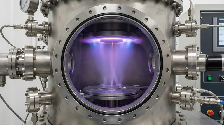
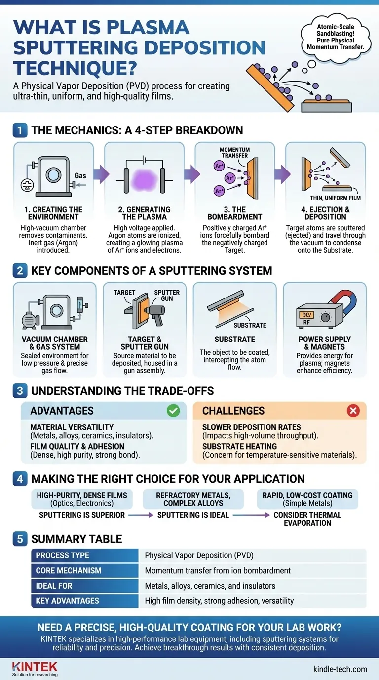
At its core, plasma sputtering is a physical vapor deposition (PVD) technique used to create exceptionally thin and uniform films on a surface. The process works by bombarding a source material, known as a target, with energized ions from a plasma. This collision physically ejects, or "sputters," atoms from the target, which then travel through a vacuum and deposit onto a substrate, forming the desired coating.
Sputtering is best understood as a form of atomic-scale sandblasting. Unlike chemical processes, it relies on pure physical momentum transfer, allowing for the deposition of a vast range of materials with high precision and strong adhesion.
The Mechanics of Plasma Sputtering: A Step-by-Step Breakdown
To truly grasp sputtering, it's essential to visualize the sequence of events that occur inside the vacuum chamber. The entire process is a carefully controlled chain reaction driven by physics.
Step 1: Creating the Environment
The process begins by placing the substrate (the object to be coated) and the target material into a high-vacuum chamber. This vacuum is critical to remove air and other contaminants that could interfere with the film's purity.
Once a vacuum is achieved, a small amount of an inert gas, almost always Argon, is introduced into the chamber.
Step 2: Generating the Plasma
A high voltage is applied within the chamber, with the target material acting as the cathode (negative electrode). This powerful electric field energizes the Argon gas, stripping electrons from the Argon atoms.
This creates a plasma, a glowing, ionized gas consisting of positive Argon ions (Ar+) and free electrons.
Step 3: The Bombardment
The positively charged Argon ions are forcefully accelerated toward the negatively charged target.
They collide with the surface of the target with immense energy. This is not a chemical reaction but a pure momentum transfer, much like a cue ball striking a rack of billiard balls.
Step 4: Ejection and Deposition
The force of the ion bombardment is strong enough to knock atoms loose from the target material. These ejected atoms travel in a straight line through the vacuum.
When these atoms reach the substrate, they condense on its surface, gradually building up a thin, uniform, and highly dense film.
Key Components of a Sputtering System
Every sputtering system relies on a few core components working in concert to achieve controlled deposition.
The Target and Sputter Gun
The target is a plate made of the material you wish to deposit. It is the source of the coating atoms and is housed in an assembly called a sputter gun.
The Substrate
The substrate is the part or material being coated. It is positioned to intercept the flow of atoms ejected from the target.
The Vacuum Chamber and Gas System
This sealed chamber provides the necessary low-pressure environment. A dedicated system controls the precise flow of Argon gas into the chamber.
The Power Supply and Magnets
A high-voltage DC or RF power supply provides the energy to create and sustain the plasma. Many modern systems also use strong magnets behind the target to confine the plasma, increasing the efficiency of the ion bombardment and deposition rate.
Understanding the Trade-offs
While powerful, sputtering is not a universal solution. Understanding its advantages and limitations is key to using it effectively.
Advantage: Material Versatility
Because it's a physical rather than chemical process, sputtering can deposit almost any material, including metals, alloys, ceramics, and insulators (using RF power). It excels at depositing complex alloys while preserving their original composition.
Advantage: Film Quality and Adhesion
Sputtered atoms arrive at the substrate with significant kinetic energy. This results in films that are extremely dense, have few impurities, and exhibit very strong adhesion to the substrate.
Challenge: Slower Deposition Rates
Compared to some other methods like thermal evaporation, sputtering can be a slower process. This can impact throughput for high-volume, low-cost applications.
Challenge: Substrate Heating
The constant energy bombardment from plasma and condensing atoms can heat the substrate. This can be a concern when coating temperature-sensitive materials like plastics.
Making the Right Choice for Your Application
Sputtering is a precision tool. Its suitability depends entirely on your end goal for the thin film.
- If your primary focus is high-purity, dense films for optics or electronics: Sputtering is the superior choice due to its exceptional control over thickness, uniformity, and film structure.
- If your primary focus is depositing refractory metals or complex alloys: Sputtering is ideal because it transfers the target material to the substrate without changing its chemical stoichiometry.
- If your primary focus is rapid, low-cost coating of simple metals: You might consider thermal evaporation, as it can offer higher deposition rates for less demanding applications.
By understanding its physical principles, you can effectively leverage plasma sputtering to engineer materials with precision at the atomic level.
Summary Table:
| Aspect | Key Detail |
|---|---|
| Process Type | Physical Vapor Deposition (PVD) |
| Core Mechanism | Momentum transfer from ion bombardment |
| Ideal For | Metals, alloys, ceramics, and insulators |
| Key Advantages | High film density, strong adhesion, material versatility |
| Common Applications | Semiconductor devices, optical coatings, wear-resistant layers |
Need a precise, high-quality coating for your lab work?
Plasma sputtering is the gold standard for creating ultra-thin, uniform films with exceptional adhesion and purity. Whether you're developing advanced electronics, durable optical coatings, or specialized wear-resistant surfaces, the right equipment is critical to your success.
At KINTEK, we specialize in high-performance lab equipment, including sputtering systems designed for reliability and precision. Our solutions help researchers and engineers like you achieve breakthrough results with consistent, repeatable deposition.
Let's discuss your specific application. Contact our experts today to find the perfect sputtering solution for your laboratory's needs.
Visual Guide
Related Products
- Chemical Vapor Deposition CVD Equipment System Chamber Slide PECVD Tube Furnace with Liquid Gasifier PECVD Machine
- RF PECVD System Radio Frequency Plasma-Enhanced Chemical Vapor Deposition RF PECVD
- 915MHz MPCVD Diamond Machine Microwave Plasma Chemical Vapor Deposition System Reactor
- Microwave Plasma Chemical Vapor Deposition MPCVD Machine System Reactor for Lab and Diamond Growth
- Cylindrical Resonator MPCVD Machine System Reactor for Microwave Plasma Chemical Vapor Deposition and Lab Diamond Growth
People Also Ask
- Why is Chemical Vapor Deposition (CVD) equipment uniquely suited for constructing hierarchical superhydrophobic structures?
- What are the advantages of chemical vapor deposition? Achieve Superior Thin Films for Your Lab
- What types of substrates are used in CVD to facilitate graphene films? Optimize Graphene Growth with the Right Catalyst
- What are the core advantages of PE-CVD in OLED encapsulation? Protect Sensitive Layers with Low-Temp Film Deposition
- How are carbon nanotubes grown? Master Scalable Production with Chemical Vapor Deposition


