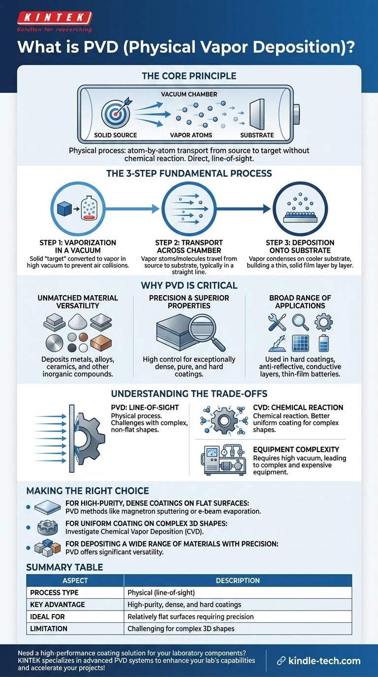
In the field of advanced manufacturing, Physical Vapor Deposition (PVD) describes a group of powerful thin film deposition techniques. These processes all operate by vaporizing a solid source material within a vacuum chamber and then depositing that vapor, atom by atom, onto the surface of a target object, known as a substrate.
The core principle of PVD is its physical nature—it transports material from a source to a target without a chemical reaction. This direct, line-of-sight process provides exceptional control over the thickness, structure, and properties of the deposited film.
The Fundamental PVD Process
At its heart, every PVD technique follows the same chronological steps to build a thin film. Understanding this sequence is key to appreciating its capabilities.
Step 1: Vaporization in a Vacuum
First, a solid source material, often called a "target," is converted into a vapor. This is done inside a high-vacuum chamber to ensure the vaporized atoms can travel without colliding with air molecules.
Step 2: Transport Across the Chamber
The vaporized atoms or molecules travel across the vacuum chamber from the source to the substrate. This journey is typically in a straight line, a characteristic that has important implications for the process.
Step 3: Deposition onto a Substrate
Finally, the vaporized material condenses on the cooler substrate, forming a thin, solid film. This film builds up layer by layer, allowing for extremely precise control over its final thickness and structure.
Why PVD is a Critical Technology
PVD is not just a laboratory technique; its unique advantages have made it a cornerstone of modern industry, enabling breakthroughs across numerous fields.
Unmatched Material Versatility
PVD can be used to deposit a vast range of materials, including metals, alloys, ceramics, and other inorganic compounds. This flexibility is a significant advantage over other methods that are limited by chemical prerequisites.
Precision and Superior Film Properties
The high degree of control in a PVD process allows for the creation of films with specific, desirable properties. These coatings can be exceptionally dense, pure, and hard, offering enhanced performance compared to the underlying substrate.
A Broad Range of Applications
The history of PVD dates back to Michael Faraday in 1838, and its modern applications are extensive. It is used for hard coatings on cutting tools, anti-reflective coatings on optics, conductive layers in semiconductor devices and solar cells, and thin-film batteries.
Understanding the Trade-offs
While powerful, PVD is not a universal solution. An objective assessment requires understanding its inherent limitations.
PVD vs. Chemical Vapor Deposition (CVD)
PVD and CVD are the two primary families of deposition techniques. The key difference is that PVD is a physical process (like sandblasting with atoms), while CVD involves a chemical reaction on the substrate's surface that produces the film. CVD can often coat complex, non-flat shapes more uniformly.
Line-of-Sight Limitations
Because PVD is a line-of-sight process, the atoms travel in a straight line from the source to the substrate. This makes it challenging to evenly coat complex three-dimensional shapes or the inside of narrow holes.
Equipment and Process Complexity
Achieving and maintaining the high vacuum required for PVD necessitates complex and expensive equipment. This can lead to higher operational costs and slower processing times compared to some non-vacuum techniques.
Making the Right Choice for Your Goal
Selecting the correct deposition method depends entirely on the desired outcome for the final product.
- If your primary focus is high-purity, dense coatings on a relatively flat surface: PVD methods like magnetron sputtering or e-beam evaporation are an excellent choice.
- If your primary focus is coating complex 3D shapes with a uniform film: You may need to investigate Chemical Vapor Deposition (CVD) as a more suitable alternative.
- If your primary focus is depositing a wide range of materials, especially metals and ceramics, with precise control: PVD offers significantly more versatility than most chemical-based methods.
Ultimately, PVD empowers engineers and scientists to construct materials atom-by-atom, enabling the advanced component performance that defines our modern world.
Summary Table:
| Aspect | Description |
|---|---|
| Process Type | Physical (line-of-sight) |
| Key Advantage | High-purity, dense, and hard coatings |
| Common Materials | Metals, alloys, ceramics |
| Ideal For | Relatively flat surfaces requiring precision |
| Limitation | Challenging for complex 3D shapes |
Need a high-performance coating solution for your laboratory components?
At KINTEK, we specialize in providing advanced lab equipment and consumables, including PVD systems, to help you achieve precise, durable thin films for your research and development. Our expertise ensures you get the right solution for depositing metals, alloys, and ceramics with exceptional control.
Contact our experts today to discuss how PVD technology can enhance your lab's capabilities and accelerate your projects!
Visual Guide
Related Products
- RF PECVD System Radio Frequency Plasma-Enhanced Chemical Vapor Deposition RF PECVD
- Split Chamber CVD Tube Furnace with Vacuum Station Chemical Vapor Deposition System Equipment Machine
- Chemical Vapor Deposition CVD Equipment System Chamber Slide PECVD Tube Furnace with Liquid Gasifier PECVD Machine
- VHP Sterilization Equipment Hydrogen Peroxide H2O2 Space Sterilizer
- 30T 40T Split Automatic Heated Hydraulic Press Machine with Heated Plates for Laboratory Hot Press
People Also Ask
- What are the advantages of PECVD? Enable Low-Temperature, High-Quality Thin-Film Deposition
- How are PECVD and CVD different? A Guide to Choosing the Right Thin-Film Deposition Process
- How does RF power create plasma? Achieve Stable, High-Density Plasma for Your Applications
- Why does PECVD commonly use RF power input? For Precise Low-Temperature Thin Film Deposition
- What is the principle of plasma enhanced chemical vapor deposition? Achieve Low-Temperature Thin Film Deposition