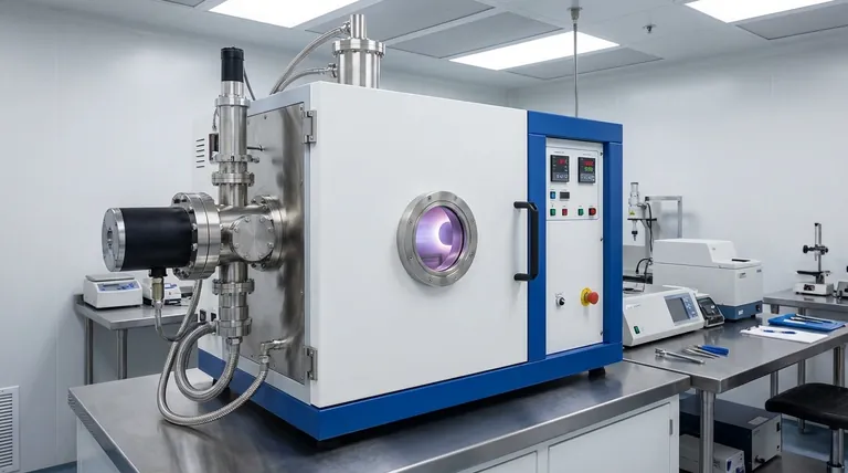
In essence, a sputtering film is an ultra-thin layer of material deposited onto a surface, atom by atom, using a high-precision physical process called sputtering. This technique, a form of physical vapor deposition (PVD), involves ejecting atoms from a source material (the "target") by bombarding it with energized ions inside a vacuum. These ejected atoms then travel and condense onto a secondary object (the "substrate"), forming a highly uniform and durable film.
Sputtering is not just about creating a thin coating; it's about engineering a surface at the atomic level. The process provides exceptional control over a film's thickness, purity, and adhesion, making it indispensable for high-performance applications like semiconductors and advanced optics.
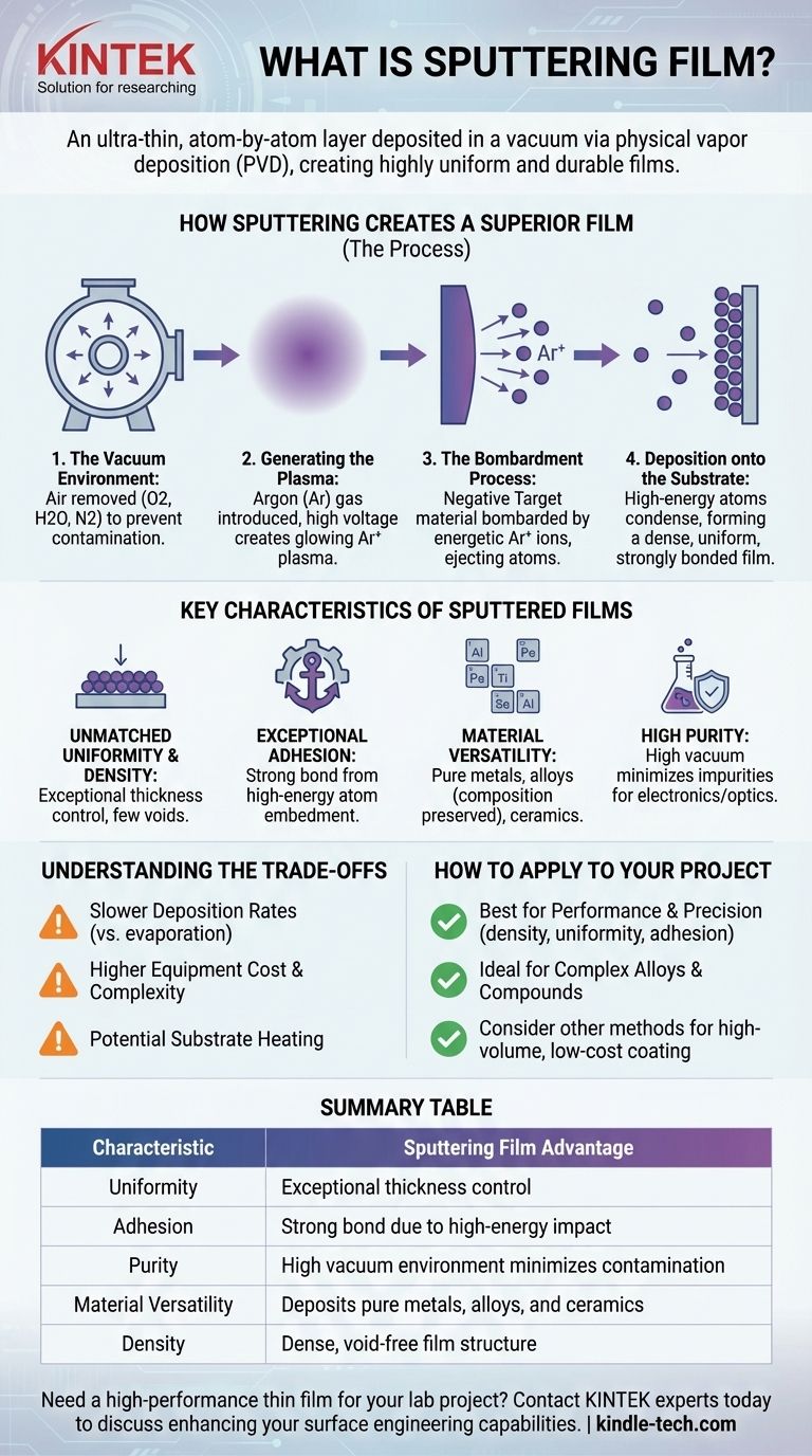
How Sputtering Creates a Superior Film
To understand the unique qualities of a sputtered film, you must first understand the mechanics of the process. It's a highly controlled sequence taking place in a vacuum.
The Vacuum Environment
First, the substrate and the target material are placed in a vacuum chamber. Air is pumped out to remove impurities like oxygen, water vapor, and nitrogen, which could otherwise contaminate the film and compromise its performance.
Generating the Plasma
A small amount of an inert gas, typically Argon, is then introduced into the chamber. A high voltage is applied, which strips electrons from the Argon atoms. This creates a glowing, energized state of matter known as plasma, consisting of positive Argon ions and free electrons.
The Bombardment Process
The target material is given a negative electrical charge. This causes the positive Argon ions from the plasma to accelerate violently towards the target. When these high-energy ions strike the target, they transfer their momentum, physically knocking out, or "sputtering," atoms from the target material.
Deposition onto the Substrate
These ejected atoms travel in straight lines through the vacuum and strike the substrate. Because these atoms arrive with significant kinetic energy, they form a very dense, uniform, and strongly bonded film as they accumulate on the substrate's surface.
Key Characteristics of Sputtered Films
The sputtering process imparts distinct advantages to the resulting film, which is why it is chosen for demanding technical applications.
Unmatched Uniformity and Density
The controlled, line-of-sight deposition results in films with exceptional thickness uniformity across the entire substrate. The energy of the arriving atoms also ensures they pack together tightly, creating a dense film with few voids or defects.
Exceptional Adhesion
The high kinetic energy of the sputtered atoms helps them physically embed into the very top layer of the substrate. This creates a much stronger bond (adhesion) between the film and the substrate compared to lower-energy processes like thermal evaporation.
Material Versatility
Sputtering can deposit a vast range of materials, including pure metals, complex alloys, and even insulating ceramic compounds. For alloys, the process does an excellent job of preserving the original composition from the target to the film.
High Purity
Because the entire process occurs in a high vacuum, the resulting film is exceptionally pure. This is a critical requirement for applications in electronics and optics, where even minute impurities can degrade performance.
Understanding the Trade-offs
Despite its advantages, sputtering is not the right choice for every application. Understanding its limitations is key to making an informed decision.
Slower Deposition Rates
Compared to other methods like thermal evaporation, sputtering is generally a slower process. The rate at which material is ejected from the target is lower, which can impact throughput in high-volume manufacturing.
Higher Equipment Cost and Complexity
Sputtering systems are sophisticated machines. The need for high-vacuum chambers, precise gas-handling systems, and specialized high-voltage power supplies makes the equipment more expensive and complex to operate and maintain.
Potential for Substrate Heating
The constant bombardment of energetic particles can transfer a significant amount of heat to the substrate. For heat-sensitive substrates, such as some plastics or biological materials, this can be a major issue that requires active cooling or alternative deposition methods.
How to Apply This to Your Project
Choosing a deposition method depends entirely on your technical requirements and budget constraints.
- If your primary focus is performance and precision: Sputtering is the superior choice when film density, uniformity, purity, and adhesion are critical for your device to function correctly.
- If your primary focus is high-volume, low-cost coating: Simpler and faster methods like thermal evaporation might be more economical for applications where the ultimate film quality is less critical.
- If you are working with complex alloys or compounds: Sputtering excels at maintaining the correct ratio of elements from the source target to the final film, a task that is difficult for other methods.
Ultimately, understanding the sputtering process allows you to select the right tool to engineer surfaces with properties that are simply not achievable otherwise.
Summary Table:
| Characteristic | Sputtering Film Advantage |
|---|---|
| Uniformity | Exceptional thickness control across the entire substrate |
| Adhesion | Strong bond due to high-energy atom impact |
| Purity | High vacuum environment minimizes contamination |
| Material Versatility | Deposits pure metals, alloys, and ceramics |
| Density | Dense, void-free film structure |
Need a high-performance thin film for your lab project?
KINTEK specializes in lab equipment and consumables for precise thin-film deposition. Our sputtering solutions deliver the uniformity, purity, and adhesion required for advanced applications in semiconductors, optics, and R&D.
Contact our experts today to discuss how we can enhance your surface engineering capabilities.
Visual Guide
Related Products
- Lab Blown Film Extrusion Three Layer Co-Extrusion Film Blowing Machine
- Lab Plastic PVC Calender Stretch Film Casting Machine for Film Testing
- Graphite Vacuum Furnace High Thermal Conductivity Film Graphitization Furnace
People Also Ask
- What is the use of a blown film machine? To Produce Strong, Versatile Plastic Films for Packaging
- What products are blown film extrusion? From Grocery Bags to Industrial Sheeting
- What is the cost of blown film extrusion? From $20K to High-End Systems
- What are the elements of blown film? Master the Key Components for High-Quality Film Production
- What is the blown film extrusion method? Master the Art of Strong, Seamless Plastic Film Production


