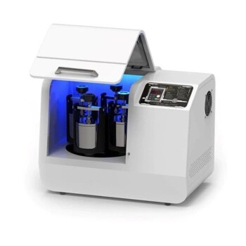
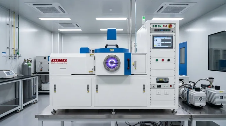
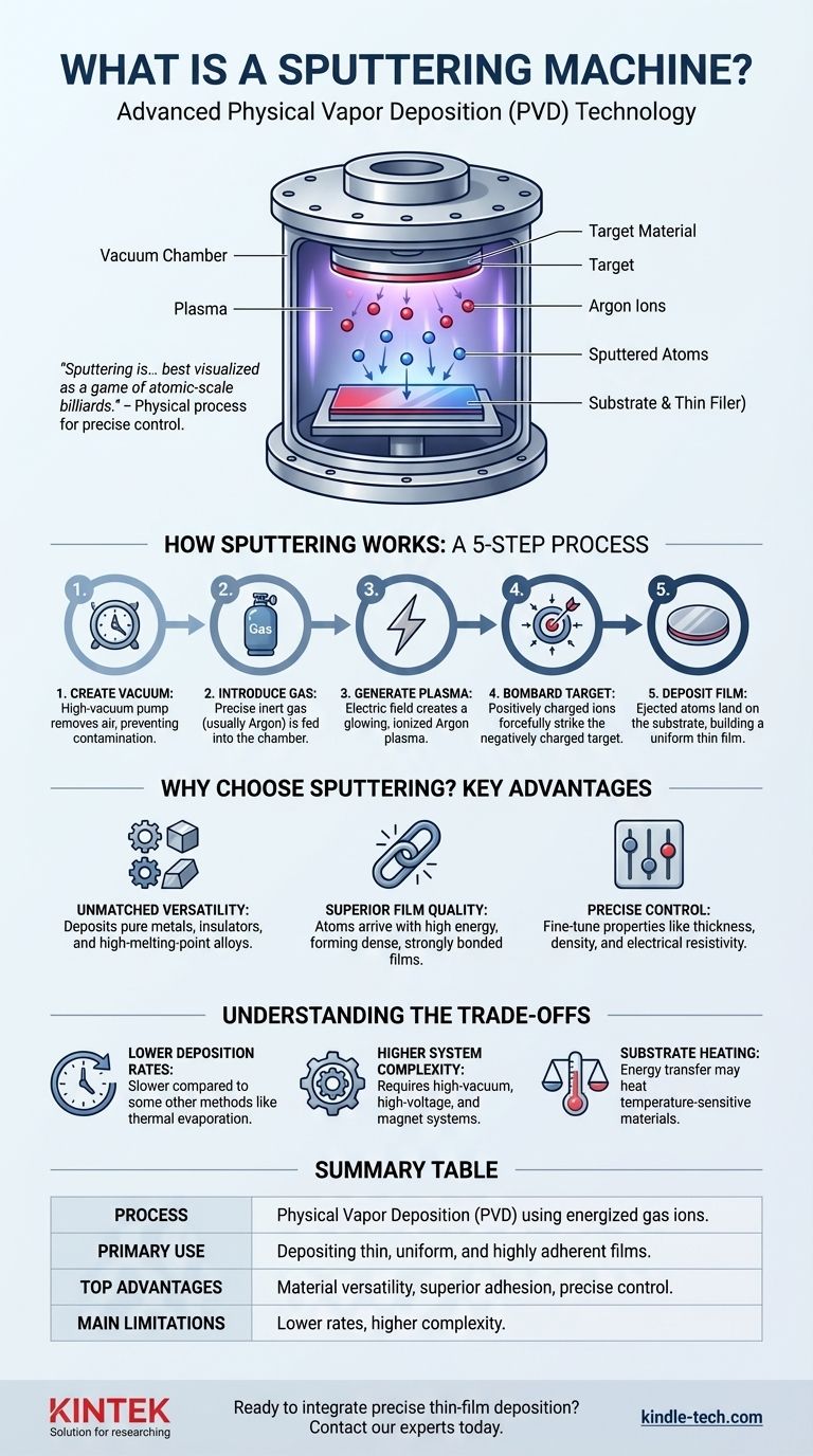
At its core, a sputtering machine is a high-tech coating system that deposits exceptionally thin layers of material onto a surface, known as a substrate. It operates inside a vacuum chamber by using energized gas ions to physically knock atoms off a source material (the "target"), which then land on the substrate to form a uniform film. This process is a form of Physical Vapor Deposition (PVD).
Sputtering is not a chemical process; it is a physical one, best visualized as a game of atomic-scale billiards. Understanding this momentum-transfer mechanism is key to grasping why it offers such precise control and is essential for depositing materials that are otherwise difficult to work with.
How Sputtering Works: A Step-by-Step Breakdown
The entire process occurs within a sealed vacuum chamber to prevent contamination and ensure the sputtered atoms can travel freely from the source to the destination.
Step 1: Creating the Vacuum
First, a powerful system of pumps removes nearly all the air from the chamber. This high-vacuum environment is critical, as it eliminates unwanted atoms and molecules that could react with or obstruct the deposition process.
Step 2: Introducing the Process Gas
A small, precisely controlled amount of an inert gas, almost always Argon, is then fed into the chamber. This gas is not part of the final coating; it serves as the "ammunition" for the process.
Step 3: Generating the Plasma
A strong electric field is applied within the chamber, with the target material being given a large negative voltage. This energy strips electrons from the Argon atoms, creating a glowing, ionized gas known as a plasma—a cloud of positively charged Argon ions and free electrons.
In modern systems, magnets are placed behind the target to trap the electrons near its surface. This magnetron sputtering intensifies the plasma, making the process much more efficient.
Step 4: The Bombardment Phase
The positively charged Argon ions in the plasma are forcefully accelerated toward the negatively charged target.
They collide with the target at high velocity. This impact has enough kinetic energy to dislodge, or "sputter," individual atoms from the target material, ejecting them into the chamber.
Step 5: Deposition on the Substrate
The sputtered atoms travel through the vacuum chamber and land on the substrate (such as a silicon wafer, glass panel, or plastic component).
These atoms gradually build up on the substrate's surface, forming a dense, uniform, and highly adherent thin film. The thickness of this film can be controlled with extreme precision.
Why Choose Sputtering? Key Advantages
Sputtering is chosen over other deposition methods for several key reasons related to control and material flexibility.
Unmatched Material Versatility
Sputtering can deposit a vast range of materials, including pure metals, insulators, and complex alloys. It excels at depositing materials with very high melting points (like tungsten or tantalum) that cannot be easily evaporated.
Because it's a physical process, it can also deposit alloys while preserving their original composition, something that is very difficult with heat-based methods.
Superior Film Quality and Adhesion
The sputtered atoms arrive at the substrate with significant kinetic energy. This energy helps them form a very dense and strongly bonded film with excellent adhesion to the substrate surface, resulting in durable and reliable coatings.
Precise Control Over Film Properties
Engineers can finely tune the final film's characteristics—such as its thickness, density, electrical resistivity, or grain structure—by precisely controlling process parameters like gas pressure, voltage, and deposition time.
Understanding the Trade-offs
While powerful, sputtering is not the universal solution for all thin-film applications. Its primary limitations must be considered.
Lower Deposition Rates
Compared to some other methods, such as thermal evaporation or certain types of Chemical Vapor Deposition (CVD), sputtering can be a slower process. This can be a factor in high-volume manufacturing where throughput is a primary concern.
Higher System Complexity
Sputtering systems require sophisticated high-vacuum pumps, high-voltage power supplies, and often complex magnet arrays. This makes the equipment more expensive and complex to maintain than simpler deposition technologies.
Potential for Substrate Heating
The energy transfer from the plasma and the condensing atoms can heat the substrate. While often manageable, this can be a limitation when coating temperature-sensitive materials like certain plastics or biological samples.
Making the Right Choice for Your Application
Selecting the correct deposition method depends entirely on your project's end goal.
- If your primary focus is material versatility and high purity: Sputtering is ideal for depositing high-melting-point metals, complex alloys, and compounds where chemical reactions are undesirable.
- If your primary focus is creating high-adhesion, dense films: The physical nature of sputtering provides excellent adhesion and film density, making it a superior choice for durable optical, electronic, or protective coatings.
- If your primary focus is high-volume throughput and lower cost: You should evaluate sputtering against faster methods like thermal evaporation, weighing the trade-off between deposition speed and final film quality.
Understanding this physical deposition mechanism empowers you to select the right tool for creating high-performance thin films with precision and control.
Summary Table:
| Aspect | Key Takeaway |
|---|---|
| Process | Physical Vapor Deposition (PVD) using energized gas ions in a vacuum. |
| Primary Use | Depositing thin, uniform, and highly adherent films onto substrates. |
| Top Advantages | Excellent material versatility, superior film adhesion, and precise control. |
| Main Limitations | Lower deposition rates and higher system complexity compared to some methods. |
Ready to integrate precise thin-film deposition into your lab's workflow?
At KINTEK, we specialize in providing high-performance sputtering machines and lab equipment tailored to your research and production needs. Our solutions deliver the material versatility and superior film quality essential for advanced electronics, optics, and protective coatings.
Contact our experts today to discuss how a KINTEK sputtering system can enhance your capabilities and drive your projects forward.
Visual Guide
Related Products
- Single Punch Manual Tablet Press Machine TDP Tablet Punching Machine
- Lab Scale Rotary Single Punch Tablet Press Machine TDP Tablet Punching Machine
- Single Punch Electric Tablet Press Machine TDP Tablet Punching Machine
- Twin Screw Extruder Plastic Granulation Machine
- Single Punch Tablet Press Machine and Mass Production Rotary Tablet Punching Machine for TDP
People Also Ask
- What is a punch tablet press? Precision Tableting for R&D and Small Batches
- What is a tablet punch? The Precision Tool Shaping Your Tablet Manufacturing
- What is the principle of a single punch tablet press machine? A Guide to Precision Lab-Scale Production
- What does a tablet punching machine consist of? Core Components for Efficient Tablet Production
- What are advantages of single punch tablet press machine? Maximize R&D Efficiency with Minimal Material