In essence, a sputtering target for semiconductors is a highly purified, solid block of material that serves as the source for depositing ultra-thin films onto a semiconductor wafer. This process, known as sputtering, is a fundamental technique for building the microscopic layers that form integrated circuits, transistors, and other electronic components. The target's material composition directly determines the properties of the deposited film.
The critical takeaway is that a sputtering target is not just raw material; it is a meticulously engineered component. Its extreme purity, density, and structural uniformity are non-negotiable requirements, as any imperfection in the target can be transferred to the semiconductor, leading to device failure.
The Role of Sputtering in Semiconductor Manufacturing
To understand the target, one must first understand the process it enables. Sputtering is a cornerstone of modern electronics manufacturing, allowing for precise, atomic-level construction.
What is Sputtering?
Sputtering is a Physical Vapor Deposition (PVD) method. Imagine a form of molecular sandblasting.
Inside a vacuum chamber, high-energy ions (typically from an inert gas like Argon) are accelerated and shot at the sputtering target.
When these ions strike the target, their momentum ejects atoms from the target's surface. These ejected atoms then travel through the vacuum and deposit onto the semiconductor wafer, forming a thin, uniform film.
Why These Thin Films are Essential
Modern microchips are built vertically, with dozens or even hundreds of layers. Each layer has a specific function—conducting electricity, insulating components, or forming a transistor gate.
Sputtering is the technique used to create many of these critical layers. The process allows for exceptional control over the film's thickness, purity, and other electrical and physical properties.
From Target to Transistor
The material from the target literally becomes part of the final microchip.
For example, a Tantalum target is used to deposit a barrier layer that prevents copper from contaminating other parts of the chip. An Indium Tin Oxide (ITO) target is used to create the transparent conductive layers essential for touch screens and flat-panel displays.
The Critical Quality Requirements of a Target
The demands placed on a sputtering target are far more stringent than for materials used in almost any other industry. This is because the semiconductor world operates at a near-atomic scale.
Purity Above All
A sputtering target must be exceptionally pure, often exceeding 99.999% purity.
Even minuscule impurities within the target can be sputtered onto the wafer, creating defects that can alter the electrical properties of the circuit or cause it to fail completely.
Structural Integrity and Uniformity
Beyond purity, the target's physical structure is critical. It must have a uniform grain size, high density, and be free of any internal voids or cracks.
A non-uniform target will sputter at an inconsistent rate, resulting in a thin film with uneven thickness across the wafer. This lack of uniformity is unacceptable for high-performance devices.
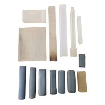
Physical Design and Form
Targets are typically flat discs or cylindrical and are bonded to a metallic holder that contains internal water-cooling channels.
The sputtering process generates significant heat, and this cooling mechanism is vital to prevent the target from overheating, cracking, or warping during operation.
Understanding the Trade-offs and Challenges
While essential, the use of sputtering targets comes with inherent complexities and considerations that engineers and managers must navigate.
The High Cost of Purity
Achieving the extreme purity and structural uniformity required for semiconductor-grade targets is an expensive and complex metallurgical process.
This makes high-quality targets a significant cost component in the overall manufacturing process. Attempting to cut costs with lower-grade targets almost always leads to lower yields and higher rates of device failure.
Material Selection is Application-Specific
There is no single "best" target material. The choice is entirely dependent on the desired function of the thin film.
Engineers must select from a wide range of materials—metals like Tantalum and Copper, alloys, and ceramic compounds like ITO—to achieve the specific conductive, insulating, or optical properties required for each layer of the device.
Process Contamination Risks
The target itself must be handled in a cleanroom environment. Any surface contamination on the target before it is placed in the sputtering chamber can be transferred to an entire batch of wafers.
This reinforces the principle that the target is a precision component, not a simple piece of raw material.
Making the Right Choice for Your Goal
Understanding the role of sputtering targets is crucial for anyone involved in the electronics value chain. Your focus will determine what aspect is most important.
- If your primary focus is materials science: The target's microstructural properties—purity, grain size, and density—are paramount as they directly dictate the performance and quality of the final thin film.
- If your primary focus is process engineering: The target's physical uniformity and design are critical for achieving consistent deposition rates, ensuring stable manufacturing, and maximizing wafer yield.
- If your primary focus is procurement or supply chain: The high cost of sputtering targets is a direct reflection of the extreme manufacturing controls needed to prevent catastrophic failures in multi-billion dollar semiconductor fabrication plants.
Ultimately, the sputtering target is the foundational source material that makes the intricate, microscopic world of modern electronics possible.
Summary Table:
| Key Attribute | Why It Matters for Semiconductors |
|---|---|
| Extreme Purity | Prevents defects and device failure; often exceeds 99.999% pure. |
| Uniform Grain Structure | Ensures consistent film thickness and deposition rate across the wafer. |
| High Density | Eliminates internal voids that could cause non-uniform sputtering. |
| Material Variety | Different materials (metals, alloys, ceramics) serve specific functions (e.g., conduction, insulation). |
Ready to integrate high-purity sputtering targets into your semiconductor manufacturing process? KINTEK specializes in providing premium lab equipment and consumables, including meticulously engineered sputtering targets designed for maximum yield and performance. Our products ensure the extreme purity and structural integrity required for your most critical applications. Contact us today to discuss how our solutions can enhance your lab's capabilities and drive your success.