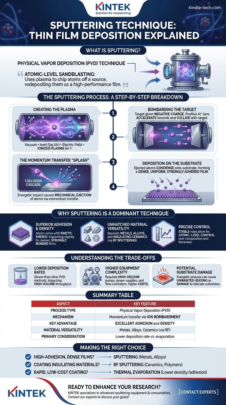
Sputtering is a physical vapor deposition (PVD) technique used to create ultra-thin, highly uniform films of material on a surface. On an atomic level, the process involves bombarding a source material, known as a "target," with high-energy ions. This bombardment physically ejects atoms from the target, which then travel through a vacuum and condense onto a "substrate," forming a thin and strongly adhered coating.
Sputtering is best understood as an atomic-level sandblasting process. Instead of sand, it uses a plasma of ionized gas to precisely chip individual atoms off a source material and redeposit them as a high-performance film onto another object.
The Sputtering Process: A Step-by-Step Breakdown
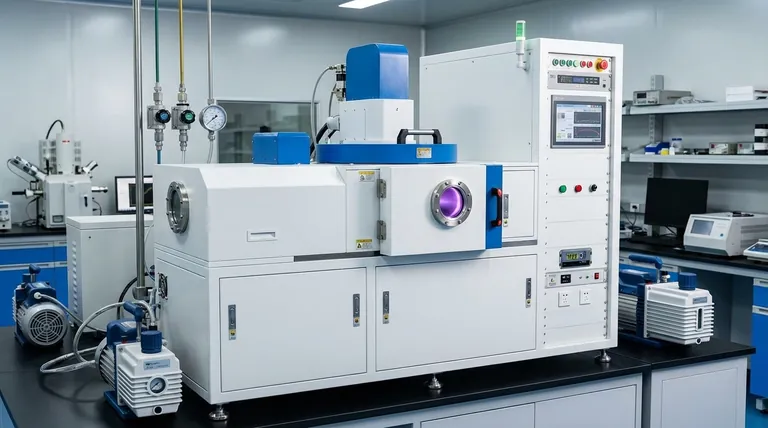
Sputtering takes place inside a vacuum chamber to ensure the purity of the film. The process is a highly controlled sequence of physical interactions rather than a chemical reaction.
Step 1: Creating the Plasma
First, the chamber is pumped down to a high vacuum and then backfilled with a small, controlled amount of an inert gas, typically Argon. A strong electric field is applied, which ionizes this gas, stripping electrons from the Argon atoms and creating a glowing, energized state of matter called a plasma.
Step 2: Bombarding the Target
This plasma contains positively charged Argon ions. The target, which is made of the material you want to deposit, is given a negative electrical charge. This potential difference causes the positive Argon ions to accelerate violently towards and collide with the negatively charged target.
Step 3: The Momentum Transfer "Splash"
When an energetic ion strikes the target, it transfers its momentum to the atoms within the target material in a collision cascade. This is not a melting or evaporation process; it is a purely mechanical ejection, much like a cue ball breaking a rack of billiard balls. The impact has enough force to knock atoms or molecules completely free from the target surface.
Step 4: Deposition on the Substrate
These ejected atoms from the target travel through the vacuum chamber and land on the substrate (e.g., a silicon wafer, glass lens, or medical implant). As they accumulate, they form a thin, dense, and highly uniform film that is securely bonded to the substrate surface.
Why Sputtering Is a Dominant Technique
Sputtering is chosen over other deposition methods for several critical advantages related to the quality and versatility of the films it produces.
Superior Film Adhesion and Density
Because sputtered atoms arrive at the substrate with significant kinetic energy, they can implant slightly into the surface and pack together very tightly. This results in films that are denser and adhere far more strongly than those produced by many other methods.
Unmatched Material Versatility
Sputtering can deposit almost any material. This includes pure metals, complex alloys, and even insulating ceramic compounds. By using a technique called RF (Radio Frequency) sputtering, it's possible to deposit non-conductive materials, a feat impossible with simpler DC sputtering setups.
Precise Control Over Composition and Thickness
The composition of a sputtered film is very close to the composition of the target material, making it ideal for depositing complex alloys. Furthermore, the deposition rate is very stable and predictable, allowing for atomic-level control over film thickness, which is critical for optical and semiconductor applications.
Understanding the Trade-offs
No technique is perfect. The precision and quality of sputtering come with specific disadvantages that must be considered.
Lower Deposition Rates
Compared to thermal evaporation, another PVD method, sputtering is generally a slower process. This can impact throughput in high-volume manufacturing environments where speed is the primary concern.
Higher Equipment Complexity
Sputtering systems are mechanically complex, requiring high-vacuum pumps, sophisticated power supplies (especially for RF), and precise gas-flow controllers. This complexity leads to higher initial equipment costs and maintenance requirements.
Potential for Substrate Damage or Heating
The energetic nature of the process can lead to unwanted heating of the substrate. For delicate substrates like polymers or certain biological samples, this energy bombardment can cause damage if not properly managed.
Making the Right Choice for Your Goal
Selecting a deposition method requires balancing film performance requirements with process constraints like cost, speed, and material compatibility.
- If your primary focus is creating high-adhesion, dense films from alloys or refractory metals: Sputtering is the superior choice due to its excellent composition control and the high energy of the deposited atoms.
- If your primary focus is coating an insulating material like a ceramic or polymer: RF Sputtering is one of the only viable and reliable techniques for producing high-quality films from non-conductive targets.
- If your primary focus is rapid, low-cost coating of a simple, low-melting-point metal: You might consider thermal evaporation, but be prepared to sacrifice the film density and adhesion that sputtering provides.
Ultimately, understanding the physical principles of sputtering empowers you to select the most effective manufacturing process for creating high-performance, precision-engineered surfaces.
Summary Table:
| Aspect | Key Feature |
|---|---|
| Process Type | Physical Vapor Deposition (PVD) |
| Mechanism | Momentum transfer via ion bombardment |
| Key Advantage | Excellent film adhesion and density |
| Material Versatility | Metals, alloys, ceramics (via RF sputtering) |
| Primary Consideration | Lower deposition rate vs. evaporation |
Ready to enhance your research with high-performance thin films? KINTEK specializes in providing advanced sputtering equipment and consumables tailored to your laboratory's specific needs. Whether you're working with metals, alloys, or insulating ceramics, our solutions deliver the precision, uniformity, and adhesion required for cutting-edge applications. Contact our experts today to discuss how we can support your thin film deposition goals!
Visual Guide
Related Products
- Spark Plasma Sintering Furnace SPS Furnace
- Vacuum Induction Melting Spinning System Arc Melting Furnace
- Chemical Vapor Deposition CVD Equipment System Chamber Slide PECVD Tube Furnace with Liquid Gasifier PECVD Machine
- Customer Made Versatile CVD Tube Furnace Chemical Vapor Deposition Chamber System Equipment
- Vacuum Cold Mounting Machine for Sample Preparation
People Also Ask
- What technical advantages does a Spark Plasma Sintering (SPS) furnace offer for LZP ceramics? Enhance Ionic Conductivity
- What is the theory of spark plasma sintering? A Guide to Rapid, Low-Temperature Densification
- What are the advantages of CAMI/SPS for W-Cu composite preparation? Reduce cycles from hours to seconds.
- What is the process fundamentals of spark plasma sintering? Achieve Rapid, High-Density Material Consolidation
- What is SPS sintering method? A Guide to High-Speed, High-Performance Material Fabrication


