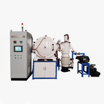
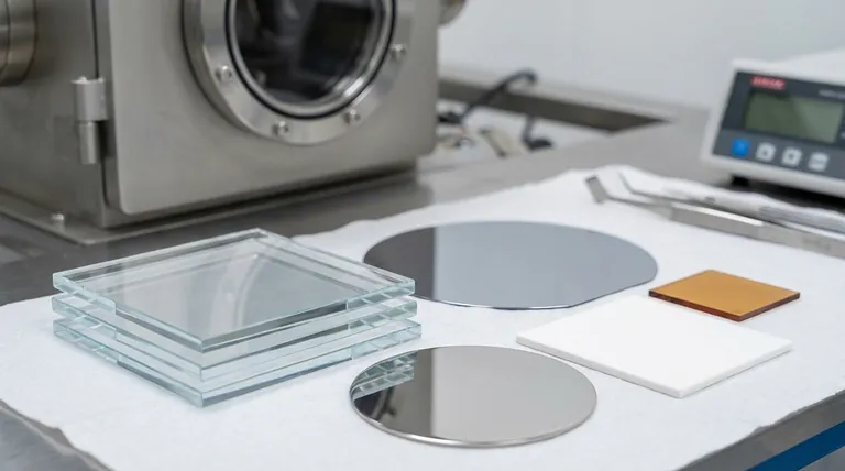
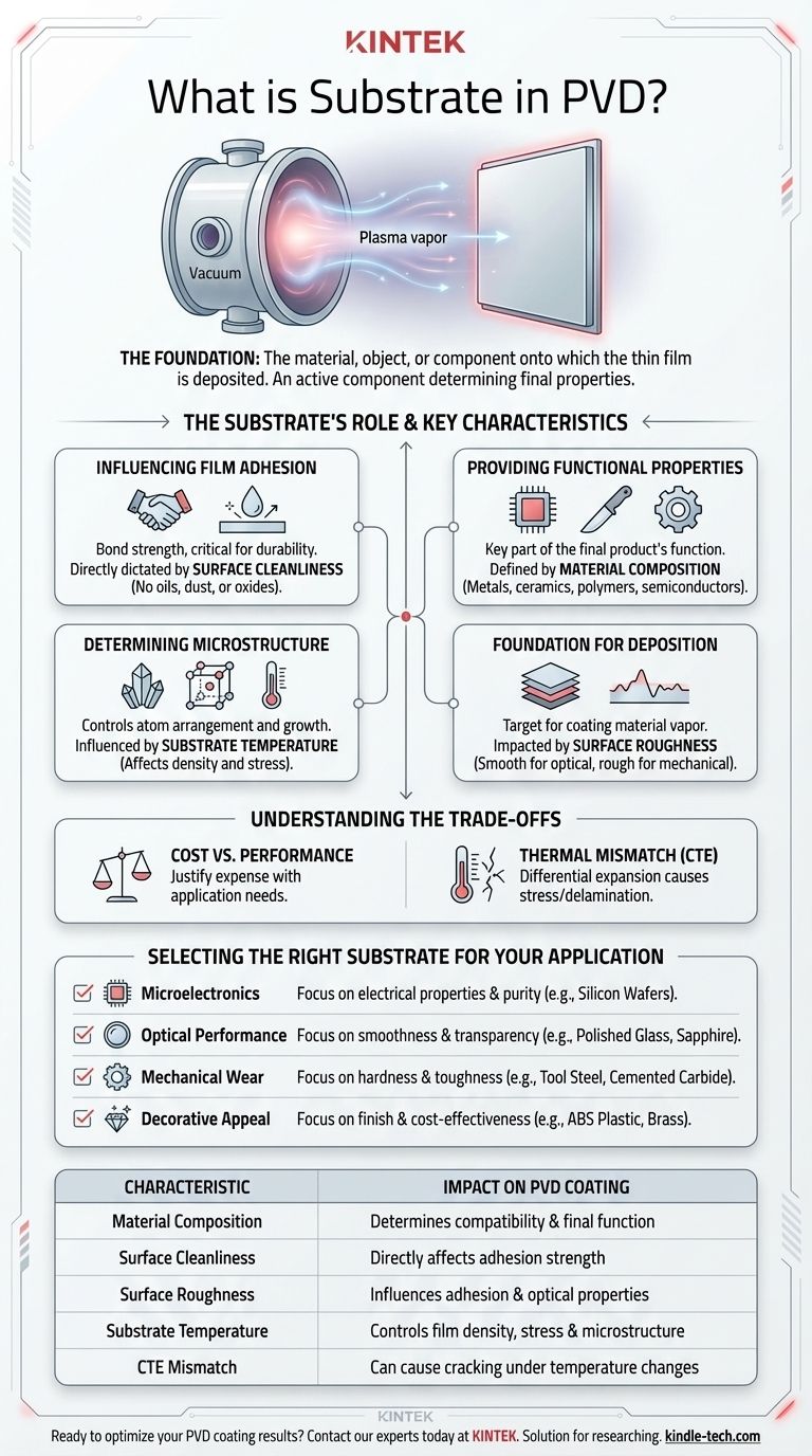
In any Physical Vapor Deposition (PVD) process, the substrate is the material, object, or component onto which the coating is deposited. It serves as the physical foundation for the thin film. While the PVD system's chamber and electronics create the coating material vapor, it is the substrate that receives this vapor and determines the final properties of the coated part.
The substrate is not merely a passive base for the coating; it is an active component whose properties—from material and temperature to surface finish—directly influence the adhesion, structure, and ultimate performance of the deposited film.
The Substrate's Role in the PVD Ecosystem
Understanding the substrate is understanding the starting point for quality. It is an integral part of the PVD process, just as critical as the coating material itself or the deposition equipment.
The Foundation for Deposition
At its most basic level, the substrate is simply the target for the vaporized coating material. Atoms or molecules travel from the source (e.g., a sputtering target) through the vacuum chamber and condense onto the substrate's surface, building the film layer by layer.
Influencing Film Adhesion
Adhesion is the bond strength between the coating and the substrate. This is arguably the most critical factor for a durable coating, and it is almost entirely dictated by the substrate's surface condition.
An unclean surface, contaminated with oils, dust, or oxides, will prevent a strong bond from forming, leading to a film that peels or flakes off easily.
Determining Microstructure and Growth
The substrate directly influences how the coating's atoms arrange themselves as they land. The substrate's temperature, for example, controls the mobility of the arriving atoms.
A hotter substrate allows atoms to move around more before settling, which can lead to a denser, less-stressed film. A colder substrate "freezes" atoms in place, which can result in a more porous or columnar structure.
Providing Functional Properties
In many applications, the substrate isn't just a holder but a key part of the final product's function. For an integrated circuit, the silicon wafer substrate is the active electronic component. For a coated turbine blade, the superalloy substrate provides the high-temperature strength.
Key Substrate Characteristics to Consider
The selection and preparation of a substrate are deliberate engineering choices. Several key characteristics must be managed to ensure a successful outcome.
Material Composition
Substrates can be made from a vast range of materials, including metals (like steel, aluminum, titanium), ceramics (alumina, silicon nitride), polymers, glass, and semiconductors (silicon wafers). The choice depends entirely on the final application's requirements.
Surface Preparation and Cleanliness
This is a non-negotiable prerequisite for good adhesion. Substrates undergo rigorous multi-step cleaning processes, often involving solvents, ultrasonic baths, and in-vacuum plasma etching immediately before deposition begins. Even a single fingerprint can ruin a coating.
Surface Roughness
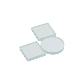
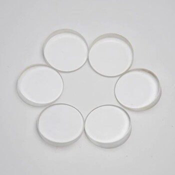
The topography, or roughness, of the substrate surface matters. An extremely smooth surface, like that on a polished silicon wafer, is essential for optical or semiconductor films. A slightly rougher surface can sometimes improve adhesion for mechanical coatings through physical interlocking.
Substrate Temperature
As mentioned, temperature is a primary process control parameter. PVD systems often include integrated heaters or cooling stages to precisely control the substrate temperature during deposition, thereby fine-tuning the film's density, stress, and crystal structure.
Understanding the Trade-offs
Choosing a substrate involves balancing competing factors. An ideal substrate for one application may be completely unsuitable for another.
Cost vs. Performance
A highly-engineered substrate, such as a large, single-crystal silicon wafer, is significantly more expensive than a simple piece of stainless steel. The cost of the substrate must be justified by the performance requirements of the application.
Thermal Mismatch
Every material has a Coefficient of Thermal Expansion (CTE)—the rate at which it expands or contracts with temperature. If the CTE of the substrate and the coating are very different, changes in temperature can build up immense stress in the film, causing it to crack or delaminate.
Chemical and Structural Compatibility
The substrate material must be stable at the required process temperatures and must not react chemically with the coating material. Furthermore, its own crystal structure can sometimes be used to influence the growth of the deposited film in a process known as epitaxy.
Selecting the Right Substrate for Your Application
The right choice is always defined by your end goal. After ensuring proper cleaning, consider the following guidelines.
- If your primary focus is microelectronics: Your choice is defined by electrical properties and purity, making single-crystal silicon wafers the standard.
- If your primary focus is optical performance: You need a substrate with exceptional smoothness and transparency in the desired wavelength, such as polished glass, fused silica, or sapphire.
- If your primary focus is mechanical wear resistance: Your substrate must be hard and tough, like tool steel or cemented carbide, where surface preparation for maximum adhesion is the top priority.
- If your primary focus is decorative appeal: Cost-effectiveness and the ability to achieve a smooth, bright finish on materials like ABS plastic, brass, or stainless steel are the main drivers.
Ultimately, a successful PVD process treats the substrate as a critical design element, not an afterthought.
Summary Table:
| Key Substrate Characteristic | Impact on PVD Coating |
|---|---|
| Material Composition (e.g., metal, ceramic, polymer) | Determines compatibility, thermal stability, and final part function |
| Surface Cleanliness | Directly affects adhesion strength; contaminants cause peeling |
| Surface Roughness | Influences film adhesion and optical properties (smooth vs. rough) |
| Substrate Temperature | Controls film density, stress, and microstructure during deposition |
| Coefficient of Thermal Expansion (CTE) | Mismatch with coating can cause cracking or delamination under temperature changes |
Ready to optimize your PVD coating results? The right substrate is just as important as the coating itself. At KINTEK, we specialize in providing high-quality lab equipment and consumables for all your PVD and surface engineering needs. Whether you're working with metals, ceramics, or semiconductors, our expertise ensures your substrates are prepared for maximum coating performance and durability. Contact our experts today to discuss how we can support your laboratory's success!
Visual Guide
Related Products
- MgF2 Magnesium Fluoride Crystal Substrate Window for Optical Applications
- Optical Window Glass Substrate Wafer Quartz Plate JGS1 JGS2 JGS3
- Float Soda-Lime Optical Glass for Laboratory Use
- Split Chamber CVD Tube Furnace with Vacuum Station Chemical Vapor Deposition System Equipment Machine
- Optical Window Glass Substrate Wafer CaF2 Substrate Window Lens
People Also Ask
- What is the substrate for CVD process? Choosing the Right Foundation for Your Thin Film
- What are the advantages of thin film substrate? Enhance Surface Functionality for Superior Products
- What substrate is used in CVD? The Foundation for High-Quality Thin Films
- What temperature can silicon carbide withstand? Operating Limits from 1600°C to 2700°C
- What is the substrate for thin film deposition? A Guide to Choosing Your Foundation