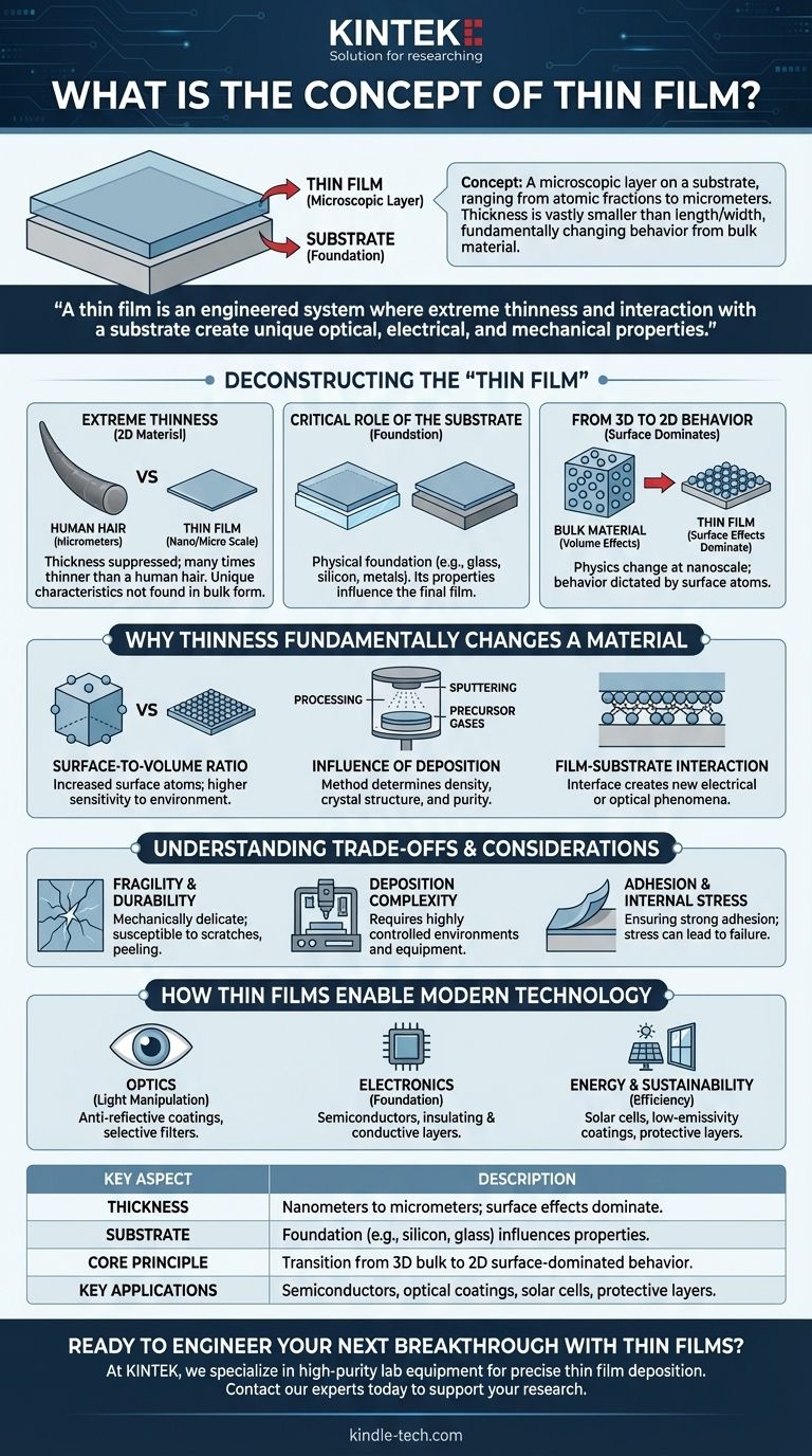
In the world of advanced materials, the concept of a thin film describes a microscopic layer of material deposited onto a surface, known as a substrate. This layer can range from a single layer of atoms (fractions of a nanometer) up to several micrometers in thickness. The defining characteristic of a thin film is that its thickness is vastly smaller than its length and width, fundamentally changing its behavior compared to a bulk piece of the same material.
A thin film is not merely a "thin version" of a material. It is an engineered system where extreme thinness and interaction with a substrate create unique optical, electrical, and mechanical properties that do not exist in the material's bulk form.
Deconstructing the "Thin Film"
To truly grasp the concept, we must look beyond the simple definition and understand its core components and principles. A thin film is defined by its scale, its foundation, and the physical reality that this combination creates.
The Defining Characteristic: Extreme Thinness
A thin film is considered a two-dimensional material because its third dimension—thickness—is suppressed to the nano or micro scale. This scale is difficult to intuit, but most thin films are many times thinner than a human hair.
This extreme thinness is the primary reason why these films possess unique characteristics not found in the bulk material.
The Critical Role of the Substrate
A thin film does not exist in isolation. It is almost always deposited onto a substrate, which acts as its physical foundation. Common substrates include glass, silicon wafers, or metals.
The substrate is not a passive base. Its own properties—such as its crystal structure, surface smoothness, and chemical composition—directly influence the final properties of the film that rests upon it.
From 3D to 2D Behavior
When a material's thickness is reduced to the nanoscale, its physics begin to change. The properties are no longer dictated by the bulk volume of atoms but by the behavior of atoms on the surface.
This is the essence of a thin film: it is a material where surface effects dominate over volume effects, opening up a new world of engineered properties.
Why Thinness Fundamentally Changes a Material
The transition from a 3D bulk material to a 2D thin film is not just a change in size; it's a change in identity. Several factors contribute to this transformation.
Surface-to-Volume Ratio
As a material becomes thinner, the ratio of atoms on its surface compared to its interior increases dramatically. This makes the film highly sensitive to its environment and amplifies properties related to its surface, such as catalytic activity or optical reflectivity.
Influence of Deposition
The method used to create the film—such as sputtering or using precursor gases in chemical deposition—has a profound impact. These techniques determine the film's density, crystal structure, and purity, directly engineering its final characteristics.
The Film-Substrate Interaction
The interface where the film meets the substrate is a critical zone. The chemical bonds and physical stresses at this boundary can create entirely new electrical or optical phenomena that neither the film material nor the substrate material possesses on its own.
Understanding the Trade-offs and Considerations
While powerful, engineering with thin films presents unique challenges. Their unique nature comes with inherent complexities that must be managed.
Fragility and Durability
By their very nature, thin films can be mechanically delicate. They are susceptible to scratches, peeling, and degradation from environmental factors if not properly designed and protected.
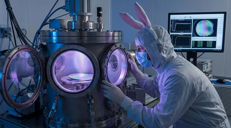
Deposition Complexity
Creating a uniform, high-purity thin film requires highly controlled environments and sophisticated equipment. Minor variations in temperature, pressure, or contaminants can ruin the film's desired properties.
Adhesion and Internal Stress
Ensuring the film adheres strongly to the substrate without cracking or delaminating is a primary engineering challenge. Stresses can build up within the film during deposition, leading to structural failure over time.
How Thin Films Enable Modern Technology
Understanding the concept of a thin film is key to understanding the technology that powers our world. Their application is tailored to manipulate light, electricity, or physical interactions at a microscopic level.
- If your primary focus is optics: Thin films are used as anti-reflective coatings on eyeglasses and camera lenses or as selective filters that block specific wavelengths of light.
- If your primary focus is electronics: They are the absolute foundation of semiconductors, forming the countless insulating, conductive, and semi-conductive layers that make up a microchip.
- If your primary focus is energy and sustainability: Thin films are critical for creating efficient solar cells, low-emissivity coatings on windows for insulation, and protective layers on tools to reduce wear.
Ultimately, mastering the thin film is about controlling matter at the nanoscale to unlock properties impossible to achieve in the bulk world.
Summary Table:
| Key Aspect | Description |
|---|---|
| Thickness | Nanometers to micrometers; surface effects dominate. |
| Substrate | Foundation (e.g., silicon, glass) that influences film properties. |
| Core Principle | Transition from 3D bulk behavior to 2D surface-dominated behavior. |
| Key Applications | Semiconductors, optical coatings, solar cells, protective layers. |
Ready to Engineer Your Next Breakthrough with Thin Films?
At KINTEK, we specialize in providing the high-purity lab equipment and consumables essential for precise thin film deposition. Whether your focus is on semiconductors, optics, or energy applications, our solutions help you achieve the uniform, durable coatings critical for success.
Contact our experts today to discuss how we can support your laboratory's thin film research and development.
Visual Guide