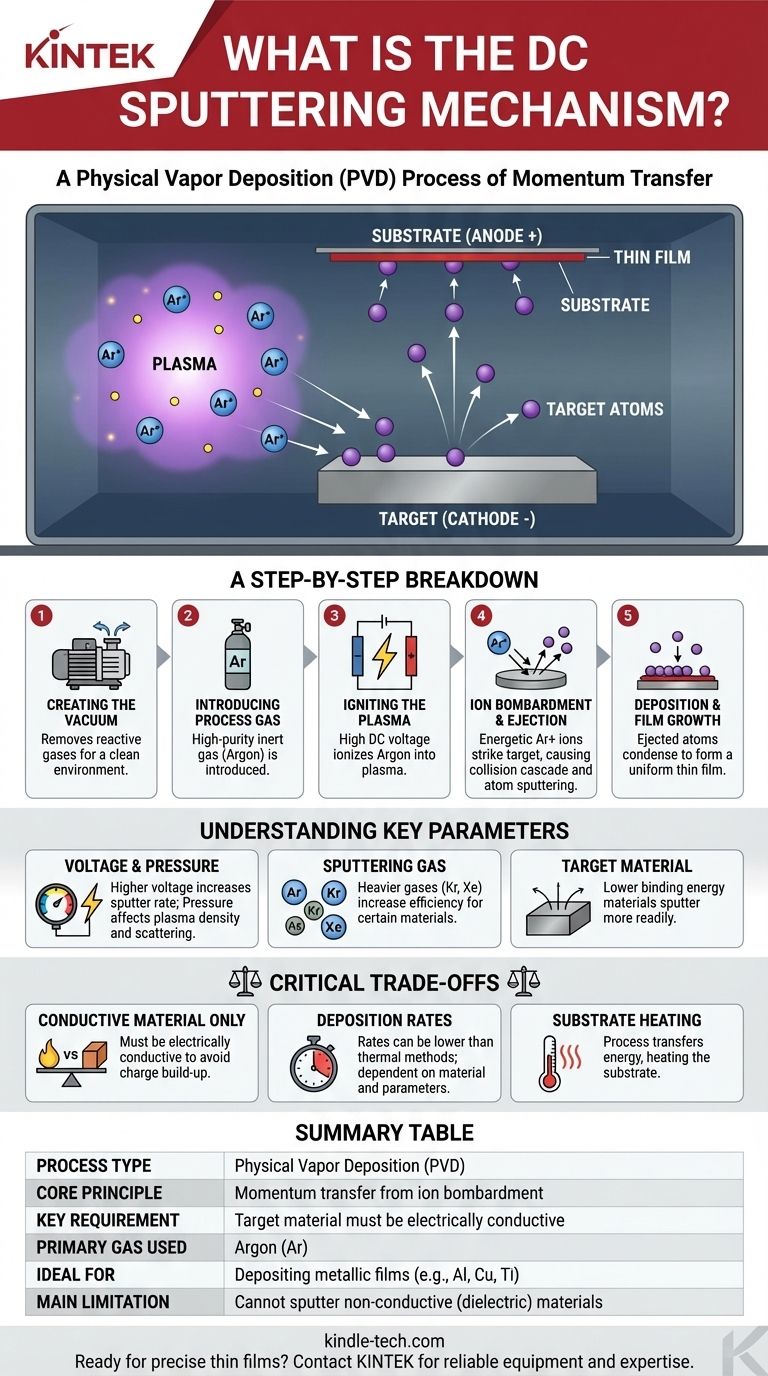
At its core, the DC sputtering mechanism is a physical vapor deposition (PVD) process that uses a plasma to create energetic ions. These ions are accelerated into a source material, known as the target, striking it with enough force to physically knock atoms loose. These ejected atoms then travel through a vacuum and deposit onto a substrate, building up a uniform thin film atom by atom.
Sputtering is not a chemical reaction or a melting process; it is a physical phenomenon of momentum transfer. Think of it as a microscopic game of billiards where gas ions act as the cue ball, knocking atoms from the target material so they can land precisely on a substrate.
A Step-by-Step Breakdown of the Mechanism
The sputtering process can be understood as a sequence of distinct physical events, each enabled by the one before it. The environment and electrical setup are critical to initiating and sustaining the mechanism.
1. Creating the Vacuum Environment
The entire process is performed inside a sealed vacuum chamber.
This initial step removes air, water vapor, and other reactive gases. A clean environment is essential for ensuring the purity of the final film and preventing unwanted chemical reactions.
2. Introducing the Process Gas
A small, controlled amount of a high-purity inert gas, most commonly Argon (Ar), is introduced into the chamber.
Argon is chosen because it is chemically non-reactive and has a suitable atomic mass to efficiently transfer momentum without forming compounds with the target material.
3. Igniting the Plasma
A high DC voltage is applied between the target and the substrate holder. The target is given a negative charge (cathode), and the substrate is typically on the grounded side of the circuit (anode).
This strong electric field energizes free electrons within the chamber, causing them to collide with and strip electrons from the neutral Argon atoms. This creates a mixture of positively charged Argon ions (Ar+) and free electrons, which is the glowing, ionized gas known as plasma.
4. Ion Bombardment and Ejection
The positively charged Ar+ ions in the plasma are strongly attracted and accelerated towards the negatively charged target.
They strike the target surface with significant kinetic energy. This impact initiates a series of internal collisions within the target material, known as a collision cascade.
When this cascade of transferred momentum reaches the surface, it overcomes the target's atomic binding energy, physically ejecting or "sputtering" atoms from the target.
5. Deposition and Film Growth
The ejected target atoms travel in a straight line through the low-pressure vacuum chamber.
When these atoms reach the substrate, they condense on its surface. Over time, these deposited atoms nucleate and grow into a continuous, dense, and highly uniform thin film.
Understanding the Key Parameters
The quality and characteristics of the final film are not accidental; they are controlled by several key process parameters that directly influence the sputtering mechanism.
The Role of Voltage and Pressure
Higher voltage increases the energy of the bombarding ions, which can increase the number of atoms sputtered per ion.
The gas pressure affects the density of the plasma and the mean free path of the sputtered atoms. Too high a pressure can cause sputtered atoms to collide with gas atoms, scattering them and reducing deposition efficiency.
The Choice of Sputtering Gas
While Argon is common, heavier inert gases like Krypton or Xenon can be used. Their greater mass allows for more efficient momentum transfer, which can increase the sputtering rate for certain materials.
The Target Material
The binding energy of the atoms in the target material directly impacts how easily they can be sputtered. Materials with lower binding energies will sputter more readily at a given ion energy.
Critical Trade-offs of DC Sputtering
While powerful, the DC sputtering mechanism has fundamental limitations that make it suitable for some applications but not others. Understanding these trade-offs is crucial for its proper use.
The Conductive Material Limitation
The most significant constraint of DC sputtering is its requirement that the target material must be electrically conductive.
A non-conductive (dielectric or insulating) target will accumulate a positive charge from the ion bombardment. This build-up neutralizes the negative bias, effectively shutting down the plasma and stopping the sputtering process.
Deposition Rates
While consistent, DC sputtering rates can be lower than some other deposition techniques, such as thermal evaporation. The rate is highly dependent on the material being sputtered and the specific process parameters used.
Substrate Heating
The constant bombardment of particles and condensing atoms transfers energy to the substrate, causing it to heat up. This can be a concern for temperature-sensitive substrates like plastics or certain biological samples.
Making the Right Choice for Your Goal
To apply this knowledge effectively, consider the nature of the material you need to deposit.
- If your primary focus is depositing a simple metallic or conductive film (like aluminum, copper, or titanium): DC sputtering is an excellent, reliable, and highly controllable choice for creating dense, high-purity films.
- If your primary focus is depositing an insulating or dielectric material (like silicon dioxide or aluminum nitride): You must use a different technique, such as RF (Radio Frequency) sputtering, which overcomes the charge build-up issue.
- If your primary focus is achieving strong adhesion and film density: The high kinetic energy of the sputtered atoms gives this process a distinct advantage over many thermal methods, resulting in superior film quality.
Understanding this mechanism transforms sputtering from a complex procedure into a predictable and powerful engineering tool for surface modification.
Summary Table:
| Key Aspect | Description |
|---|---|
| Process Type | Physical Vapor Deposition (PVD) |
| Core Principle | Momentum transfer from ion bombardment to eject target atoms |
| Key Requirement | Target material must be electrically conductive |
| Primary Gas Used | Argon (Ar) |
| Ideal For | Depositing metallic films (e.g., Al, Cu, Ti) |
| Main Limitation | Cannot sputter non-conductive (dielectric) materials |
Ready to achieve precise, high-quality thin films for your laboratory?
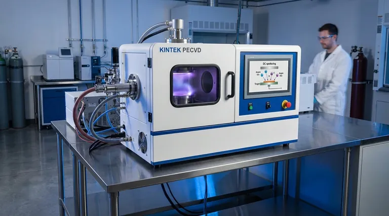
Understanding the DC sputtering mechanism is the first step. Implementing it effectively requires the right equipment and expertise. KINTEK specializes in providing reliable lab equipment and consumables for all your Physical Vapor Deposition needs.
Our team can help you select the ideal sputtering system to deposit uniform, dense conductive films for your specific application. Contact us today to discuss your project and discover how our solutions can enhance your research and development.
Get in touch via our Contact Form to speak with an expert!
Visual Guide
Related Products
- Spark Plasma Sintering Furnace SPS Furnace
- Multi Heating Zones CVD Tube Furnace Machine Chemical Vapor Deposition Chamber System Equipment
- Vacuum Induction Melting Spinning System Arc Melting Furnace
- Circulating Water Vacuum Pump for Laboratory and Industrial Use
People Also Ask
- Why are Spark Plasma Sintering (SPS) furnaces or hot presses utilized in the preparation of Li3PS4 solid electrolytes?
- What is the mechanism of SPS process? A Deep Dive into Rapid, Low-Temperature Sintering
- What is the pressure for spark plasma sintering? A Guide to Optimizing SPS Parameters
- What are the advantages of CAMI/SPS for W-Cu composite preparation? Reduce cycles from hours to seconds.
- What is the difference between spark plasma sintering and flash sintering? A Guide to Advanced Sintering Methods


