In fabrication, deposition is the process of applying a thin film of material onto a surface, known as a substrate. It is a foundational "additive" technique used across numerous industries, from semiconductor manufacturing to aerospace engineering, where materials are built up layer by layer on a molecular or atomic scale.
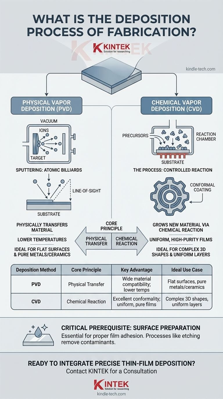
Deposition is not a single process, but a category of techniques used to add material to a workpiece. The fundamental choice is between Physical Vapor Deposition (PVD), which physically transfers material, and Chemical Vapor Deposition (CVD), which grows a new material on the surface via a chemical reaction.
The Core Principle: Building from the Atom Up
Deposition is the counterpart to "subtractive" processes like etching or milling, which remove material. Instead of carving a block of material down to the desired shape, deposition builds the desired features up from nothing.
This method is essential for creating components where extremely thin, pure, or specialized layers are required. These layers can provide electrical conductivity, insulation, wear resistance, optical properties, or corrosion protection.
Two Fundamental Approaches: Physical vs. Chemical
All deposition techniques fall into one of two major families based on how the material arrives at the substrate.
- Physical Deposition: In this approach, the source material is physically moved from a source to the substrate without a chemical change. Think of it like spray painting, where particles of paint are transported from the can to the wall.
- Chemical Deposition: In this approach, gaseous chemical precursors are introduced into a chamber. They react on the substrate's surface to form a completely new solid material. This is more like rust forming on iron—a chemical reaction on the surface creates a new layer.
Understanding Physical Vapor Deposition (PVD)
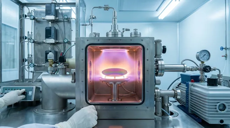
PVD processes take place in a vacuum to ensure the path from the material source to the substrate is clear of contaminants.
Sputtering: Atomic Billiards
Sputtering is a highly versatile PVD technique. A solid "target" of the desired coating material is bombarded with high-energy ions inside a vacuum chamber.
This bombardment acts like a subatomic game of pool, knocking atoms loose from the target. These freed atoms then travel through the vacuum and deposit onto the substrate, forming a thin, dense film.
Spraying: A Direct Transfer
In its simplest form, physical deposition can also involve spraying fine particles or droplets of a material directly onto the substrate. While less precise than vacuum-based methods, it serves specific industrial coating applications.
Understanding Chemical Vapor Deposition (CVD)
CVD is a process defined by the creation of a solid film through a controlled chemical reaction on a heated substrate.
The Process: A Controlled Reaction
A workpiece is placed in a reaction chamber, and specific gases (precursors) are introduced. The heat of the substrate energizes these gases, causing them to react and decompose on the surface.
This reaction leaves behind a solid film of the desired material, and the gaseous byproducts are vented away. The vacuum environment helps pull the reactant gases to the workpiece and ensures purity.
Why Choose CVD?
CVD is prized for its ability to create exceptionally pure and uniform films. Because the gas precursors flow around the entire workpiece, CVD can produce highly conformal coatings that perfectly cover even complex, three-dimensional shapes with an even thickness.
Understanding the Trade-offs
The choice between PVD and CVD is dictated by the material, the substrate, and the desired properties of the final film.
PVD: The Direct Approach
PVD methods like sputtering are excellent for depositing a very wide range of materials, including metals, alloys, and ceramics that are difficult to vaporize chemically. They are often run at lower temperatures than CVD, which is safer for sensitive substrates.
However, PVD is a "line-of-sight" process. It can struggle to evenly coat the hidden surfaces or complex internal geometries of a 3D object.
CVD: The Conformal Approach
CVD's primary advantage is its excellent conformality. It is the superior choice for creating uniform films over intricate topographies, which is critical in microelectronics.
The main trade-offs are the high temperatures often required, which can damage the substrate, and the use of precursor gases that can be complex, expensive, or hazardous.
A Critical Prerequisite: Surface Preparation
No deposition process will succeed without a perfectly clean surface. Processes like etching are not deposition methods; they are subtractive pre-treatments used to remove oxides and other contaminants. This ensures the deposited film adheres properly to the substrate.
Choosing the Right Deposition Method
Your decision should be guided by the specific requirements of your component.
- If your primary focus is coating a simple, flat surface with a pure metal: PVD methods like sputtering are often the most direct and cost-effective solution.
- If your primary focus is creating a highly uniform, crystalline film on a complex 3D shape: CVD is superior due to its ability to conformally coat all surfaces.
- If your primary focus is applying a hard, wear-resistant coating onto a heat-sensitive tool: A low-temperature PVD process is frequently the ideal choice.
Ultimately, understanding the distinction between physically moving a material and chemically creating it is the key to selecting the right tool to build your product from the atom up.
Summary Table:
| Deposition Method | Core Principle | Key Advantage | Ideal Use Case |
|---|---|---|---|
| Physical Vapor Deposition (PVD) | Physically transfers material from a source to the substrate. | Wide material compatibility; lower temperatures. | Coating flat surfaces with pure metals or ceramics. |
| Chemical Vapor Deposition (CVD) | Grows a new material on the surface via a chemical reaction. | Excellent conformality; uniform, high-purity films. | Coating complex 3D shapes with highly uniform layers. |
Ready to integrate precise thin-film deposition into your fabrication process?
The right deposition technique is critical for achieving the electrical, optical, or protective properties your product requires. At KINTEK, we specialize in providing high-quality lab equipment and consumables for deposition processes, including PVD and CVD systems.
Our experts can help you select the ideal solution for your specific materials and substrate needs, ensuring superior film quality and performance. Contact us today to discuss how our deposition technologies can advance your laboratory's capabilities.
Contact KINTEK for a Consultation
Visual Guide
Related Products
- Chemical Vapor Deposition CVD Equipment System Chamber Slide PECVD Tube Furnace with Liquid Gasifier PECVD Machine
- RF PECVD System Radio Frequency Plasma-Enhanced Chemical Vapor Deposition RF PECVD
- Inclined Rotary Plasma Enhanced Chemical Vapor Deposition PECVD Equipment Tube Furnace Machine
- Evaporation Boat for Organic Matter
- Hemispherical Bottom Tungsten Molybdenum Evaporation Boat
People Also Ask
- What is the chemical vapor deposition growth process? Build Superior Thin Films from the Atom Up
- Why is Chemical Vapor Deposition (CVD) equipment uniquely suited for constructing hierarchical superhydrophobic structures?
- How expensive is chemical vapor deposition? Understanding the True Cost of High-Performance Coating
- What are the core advantages of PE-CVD in OLED encapsulation? Protect Sensitive Layers with Low-Temp Film Deposition
- What are the processes of vapor phase deposition? Understand CVD vs. PVD for Superior Thin Films


