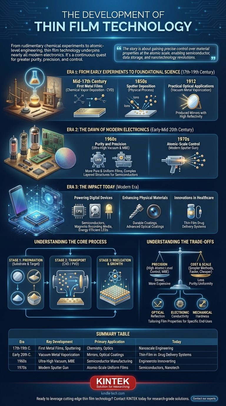
The development of thin film technology is a centuries-long journey from rudimentary chemical experiments to the atomic-level engineering that underpins nearly all modern electronics. Its history tracks a continuous quest for greater purity, precision, and control, beginning with metal film creation in the mid-17th century, progressing to sputter deposition in the 1850s, and culminating in today's advanced techniques that create layers mere nanometers thick.
The story of thin film is not just about making things thinner. It's about gaining precise control over material properties at the atomic scale, a capability that has directly enabled the semiconductor, data storage, and nanotechnology revolutions.
From Early Experiments to Foundational Science
The origins of thin film technology were not driven by electronics, but by chemistry and optics. Early researchers were simply exploring how to coat one material with a very thin layer of another.
The 17th-19th Century: The First Depositions
The first documented creation of metal films occurred in the mid-17th century using a process that would become known as chemical vapor deposition (CVD).
Experiments with oxide deposition followed around 1760. The 19th century brought another key breakthrough with the first steps in sputter deposition in the 1850s, a physical process that uses ions to dislodge atoms from a target material onto a substrate.
The Early 20th Century: Practical Optical Applications
The first significant use of thin films for a practical optical purpose came in 1912, when scientists produced mirrors by vaporizing metals like silver and aluminum in a high vacuum.
By the 1930s, this process was refined for manufacturing, with early-stage thin films being used to create high-reflectivity mirrors on a larger scale.
The Dawn of Modern Electronics
The second half of the 20th century transformed thin film from a niche optical and chemical process into a cornerstone of the electronics industry. This shift was driven by the demand for smaller, more powerful components.
The 1960s Revolution: Purity and Precision
The 1960s were a pivotal decade. The development of ultra-high vacuum technology and in-situ electron microscopy allowed for the creation of far more pure and uniform films.
This period also saw the invention of molecular beam epitaxy (MBE), a highly precise deposition method developed specifically for manufacturing the complex, layered structures required for semiconductors.
The 1970s: Atomic-Scale Control
In 1970, the invention of the modern sputter gun enabled the deposition of films with atomic-scale uniformity. This device uses ion and electron collisions to deposit material with unprecedented control, a technique still fundamental to the industry today.
Understanding the Core Process
Regardless of the specific technique, the growth of a thin film follows a fundamental three-step sequence, typically occurring inside a vacuum chamber.
The Three Stages of Film Growth
First, the process begins by preparing the substrate (the base material) and the target material that will form the film.
Second, the target material is transported to the substrate. This is the stage where techniques like CVD (using chemical reactions) or PVD (using physical means like sputtering) differ.
Finally, the transported material nucleates and grows on the substrate surface, forming the desired thin film layer by layer.
Understanding the Trade-offs: Why So Many Methods?
The historical development of numerous deposition methods was not accidental. It was driven by the need to create films with specific, highly-tuned properties for different applications. The choice of method involves critical trade-offs.
The Goal: Tailoring Film Properties
A thin film's final characteristics are dictated by its end-use. Its requirements can be optical (like a mirror's reflectivity), electronic (like a semiconductor's conductivity), mechanical (like a cutting tool's hardness), or chemical.
Often, a single film must meet demanding requirements in multiple categories simultaneously, which requires a highly controlled deposition process.
The Challenge: Control vs. Cost and Scale
More advanced techniques like molecular beam epitaxy offer incredible atomic-level precision, but they are often slower and more expensive.
Older, simpler methods may be faster and cheaper for creating basic coatings, but they lack the purity and uniformity required for high-performance electronics. The evolution of thin film technology is a continuous effort to balance precision, material properties, and manufacturing cost.
The Impact of Thin Film Technology Today
Thin films are an invisible but essential component of the modern world, enabling technological breakthroughs across numerous fields.
Powering Digital Devices
Thin film deposition is the foundation of the semiconductor industry, used to build microprocessors. It is also critical for creating magnetic recording media for hard drives, integrated circuits, and energy-efficient LEDs.
Enhancing Physical Materials
Beyond electronics, thin films provide critical functions as durable, hard coatings on cutting tools to increase their lifespan. They are also used to create advanced optical coatings for lenses, filters, and high-performance glass.
Innovations in Healthcare
The principles of thin film are even being applied in medicine, with the development of thin-film drug delivery systems that allow for controlled release of medication.
Making Sense of the Evolution
Understanding the development of thin film technology provides a clear framework for its application. Your takeaway depends on your goal.
- If your primary focus is historical context: The evolution was a clear progression from creating simple macro-scale coatings to achieving precise atomic-level engineering.
- If your primary focus is manufacturing: The choice of deposition method (e.g., CVD vs. PVD/sputtering) is a critical trade-off between the required film properties, precision, and production cost.
- If your primary focus is future innovation: The next frontier lies in using these techniques to create and manipulate materials at the nano-scale, unlocking entirely new electronic, optical, and physical properties.
Ultimately, thin film technology is the invisible architecture that enables the performance, miniaturization, and functionality of our most advanced tools.
Summary Table:
| Era | Key Development | Primary Application |
|---|---|---|
| 17th-19th Century | First Metal Films (CVD), Sputtering | Chemistry, Optics |
| Early 20th Century | Vacuum Metal Vaporization | Mirrors, Optical Coatings |
| 1960s | Ultra-High Vacuum, MBE Invention | Semiconductor Manufacturing |
| 1970s | Modern Sputter Gun | Atomic-Scale Uniform Films |
| Today | Nanoscale Engineering | Semiconductors, Data Storage, Nanotech |
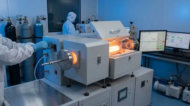
Ready to leverage cutting-edge thin film technology in your lab?
KINTEK specializes in providing the advanced lab equipment and consumables needed for precise thin film deposition, from research-grade sputtering systems to CVD reactors. Whether you are developing next-generation semiconductors, optical coatings, or nanomaterials, our solutions deliver the purity, control, and reliability required for groundbreaking work.
Contact our thin film experts today to discuss how we can support your specific application and help you achieve superior results.
Visual Guide
Related Products
- Aluminized Ceramic Evaporation Boat for Thin Film Deposition
- Tungsten Evaporation Boat for Thin Film Deposition
- Electron Beam Evaporation Coating Oxygen-Free Copper Crucible and Evaporation Boat
- Molybdenum Tungsten Tantalum Evaporation Boat for High Temperature Applications
- HFCVD Machine System Equipment for Drawing Die Nano-Diamond Coating
People Also Ask
- What is the source of evaporation for thin film? Choosing Between Thermal and E-Beam Methods
- What is thin film deposition? Unlock Advanced Surface Engineering for Your Materials
- Why is an alumina boat and Ti3AlC2 powder bed necessary for Ti2AlC sintering? Protect MAX Phase Purity
- What are the alternatives to sputtering? Choose the Right Thin Film Deposition Method
- What are thin films deposited by evaporation? A Guide to High-Purity Coating


