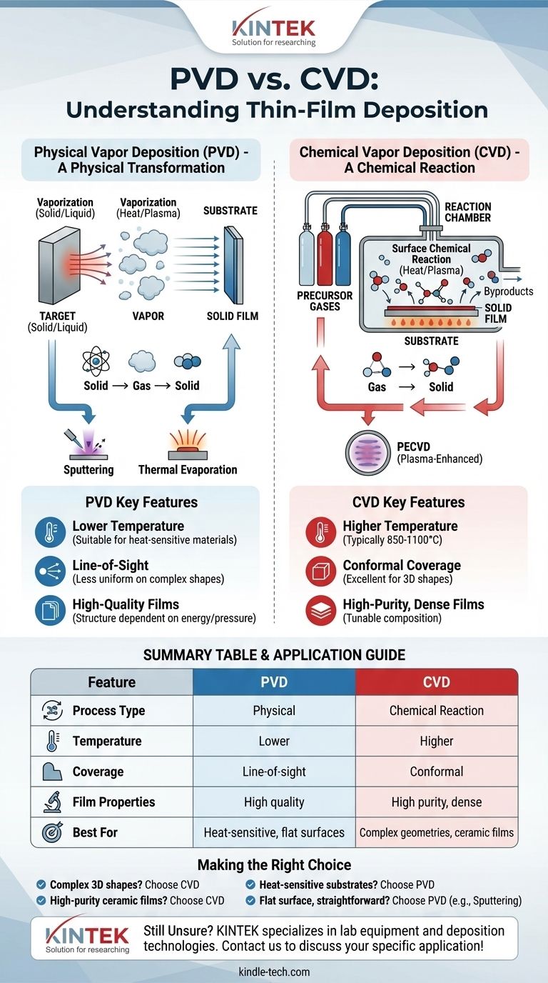
The fundamental difference between Chemical Vapor Deposition (CVD) and Physical Vapor Deposition (PVD) lies in how the coating material travels to the substrate. In PVD, the material starts as a solid, is physically vaporized into a gas, and then deposits on the part. In CVD, the material starts as a precursor gas which undergoes a chemical reaction on the substrate’s surface to form the solid film.
The core distinction is one of process: PVD is a physical transformation (solid to gas to solid), whereas CVD is a chemical reaction (gas to solid). This single difference dictates the temperature, applications, and types of surfaces each method is suited for.
Demystifying Physical Vapor Deposition (PVD)
PVD encompasses a set of vacuum deposition methods that use physical processes to produce a vapor of material, which then condenses on the object to be coated. Think of it as a highly controlled, atomic-level spray painting.
The Core Principle: Physical Transition
In PVD, the material to be deposited starts in a solid or liquid form, often called a "target." Energy is applied in a vacuum to turn this source material into a vapor, which then travels in a straight line to coat the substrate.
Key Method 1: Sputtering
Sputtering uses a high-energy source, typically a plasma, to bombard the solid target material. This bombardment physically dislodges or "sputters" atoms from the target, which then travel through the vacuum chamber and deposit onto the substrate.
Key Method 2: Thermal Evaporation
This method uses high temperatures in a vacuum to heat the source material until it boils and evaporates (or sublimes directly from a solid to a gas). This vapor then travels through the chamber and condenses on the cooler surface of the substrate, forming a thin film.
Understanding Chemical Vapor Deposition (CVD)
CVD is a process where a substrate is exposed to one or more volatile precursor gases, which react and/or decompose on the substrate surface to produce the desired solid deposit.
The Core Principle: Surface Chemical Reaction
In CVD, the process begins with gases, not solids. These precursor gases are introduced into a reaction chamber containing the heated substrate. The heat provides the energy needed to trigger a chemical reaction on the substrate's surface.
The Result: A New Solid Film
This reaction forms a new, solid material layer directly on the substrate. Unreacted precursor gases and chemical byproducts are then pumped out of the chamber, leaving behind a pure and dense film.
Common Variations: Lowering the Temperature
Variations like Plasma-Enhanced Chemical Vapor Deposition (PECVD) use plasma to provide the energy for the chemical reaction. This allows the process to run at significantly lower temperatures, making it suitable for substrates that cannot withstand the intense heat of traditional CVD.
Understanding the Key Differences and Trade-offs
The choice between PVD and CVD is driven by critical trade-offs in temperature, geometry, and desired film properties.
Deposition Temperature
CVD typically requires very high temperatures, often between 850-1100°C, to drive the necessary chemical reactions. This severely limits the types of substrate materials that can be coated without being damaged.
PVD generally operates at much lower temperatures, making it suitable for a wider range of materials, including heat-sensitive plastics and certain alloys.
Conformal Coverage (The "Wrap-Around" Effect)
CVD excels at coating complex, 3D shapes uniformly. Because the process uses gases that flow around the part, it has excellent "wrap-around" properties, resulting in a consistent film thickness even on intricate surfaces.
PVD is primarily a line-of-sight process. The vaporized material travels in a straight line from the source to the substrate, making it difficult to evenly coat undercuts, sharp corners, or the inside of hollow parts without complex part rotation.
Film Purity and Structure
CVD is renowned for producing exceptionally high-purity and dense films. By precisely controlling the mixture of precursor gases, operators can finely tune the film's chemical composition, crystal structure, and grain size.
PVD also produces high-quality films, but the control mechanisms are different. The film structure is more dependent on factors like deposition pressure and energy, and it can be more challenging to create complex alloyed films compared to CVD.
Making the Right Choice for Your Application
Selecting the correct deposition method requires matching the process capabilities to your project's specific goals.
- If your primary focus is coating complex 3D shapes uniformly: CVD is the superior choice due to its non-line-of-sight nature and excellent conformal coverage.
- If you are working with heat-sensitive substrates like plastics or certain alloys: PVD is the necessary choice because of its significantly lower processing temperatures.
- If your goal is an extremely high-purity, crystalline, or ceramic film: CVD often provides unparalleled control over the film's chemical composition and structural properties.
- If you need a straightforward, line-of-sight deposition for a flat surface (e.g., in optics or semiconductors): PVD methods like sputtering are an industry standard, offering reliable and efficient coating.
Ultimately, the choice between PVD and CVD depends entirely on the material properties, substrate limitations, and surface geometry of your specific application.
Summary Table:
| Feature | PVD (Physical Vapor Deposition) | CVD (Chemical Vapor Deposition) |
|---|---|---|
| Process Type | Physical transformation (solid → gas → solid) | Chemical reaction (gas → solid) |
| Temperature | Lower (suitable for heat-sensitive substrates) | Higher (typically 850-1100°C) |
| Coverage | Line-of-sight (less uniform on complex shapes) | Conformal (excellent for 3D shapes) |
| Film Properties | High quality, structure dependent on energy/pressure | High purity, dense, tunable composition |
| Best For | Heat-sensitive materials, flat surfaces | Complex geometries, high-purity ceramic films |
Still unsure whether PVD or CVD is right for your lab's thin-film coating needs?
KINTEK specializes in lab equipment and consumables, serving laboratory needs with expert guidance on deposition technologies. Our team can help you select the ideal system based on your substrate material, desired film properties, and geometric requirements.
Contact us today via our contact form to discuss your specific application and discover how our solutions can enhance your research or production process!
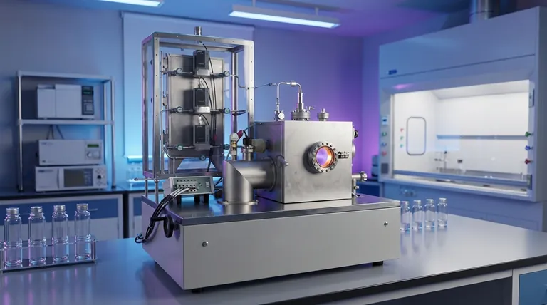
Visual Guide
Related Products
- Chemical Vapor Deposition CVD Equipment System Chamber Slide PECVD Tube Furnace with Liquid Gasifier PECVD Machine
- RF PECVD System Radio Frequency Plasma-Enhanced Chemical Vapor Deposition RF PECVD
- Microwave Plasma Chemical Vapor Deposition MPCVD Machine System Reactor for Lab and Diamond Growth
- Customer Made Versatile CVD Tube Furnace Chemical Vapor Deposition Chamber System Equipment
- 915MHz MPCVD Diamond Machine Microwave Plasma Chemical Vapor Deposition System Reactor
People Also Ask
- What are the advantages of chemical vapor deposition? Achieve Superior Thin Films for Your Lab
- What is plasma enhanced chemical vapor deposition PECVD equipment? A Guide to Low-Temperature Thin Film Deposition
- What are the core advantages of PE-CVD in OLED encapsulation? Protect Sensitive Layers with Low-Temp Film Deposition
- What is the chemical vapor deposition growth process? Build Superior Thin Films from the Atom Up
- What are the processes of vapor phase deposition? Understand CVD vs. PVD for Superior Thin Films


