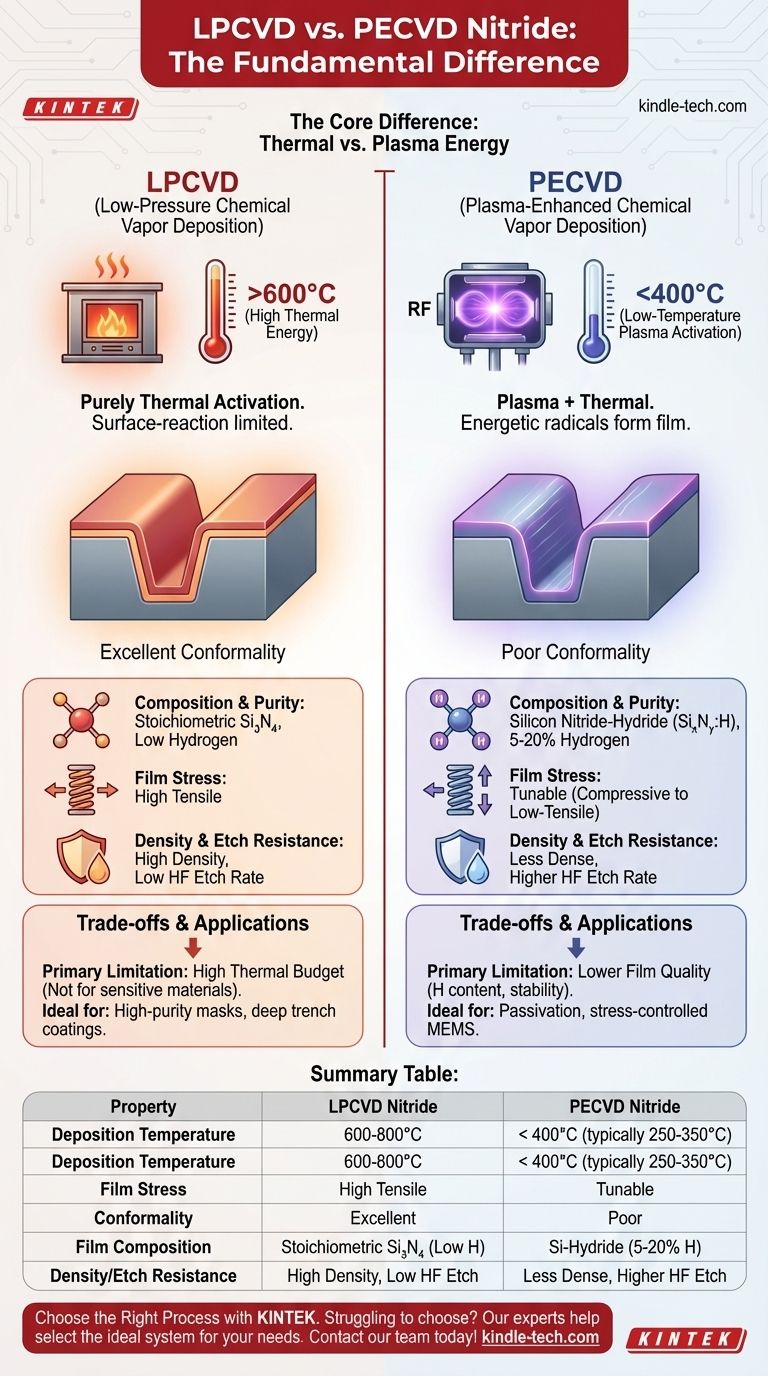
The fundamental difference between LPCVD and PECVD nitride is the energy source used for the deposition reaction. Low-Pressure Chemical Vapor Deposition (LPCVD) relies purely on high thermal energy (600-800°C) to break down precursor gases. In contrast, Plasma-Enhanced Chemical Vapor Deposition (PECVD) uses an electrical field to generate a plasma, allowing the reaction to occur at much lower temperatures (typically under 400°C).
This choice is not about which process is "better," but which is appropriate for the task. The decision hinges on a critical trade-off: LPCVD offers superior film quality and conformality at the cost of a high thermal budget, while PECVD provides low-temperature processing and stress control at the cost of lower film purity and density.
The Core Difference: Thermal vs. Plasma Energy
The method used to supply energy to the chemical reaction dictates every major difference between the resulting silicon nitride films.
LPCVD: High-Temperature Thermal Activation
LPCVD processes rely exclusively on heat to drive the chemical reaction. Substrates are placed in a furnace and heated to temperatures often exceeding 700°C.
At these high temperatures, precursor gases (typically dichlorosilane and ammonia) have enough thermal energy to react on the substrate surface, forming a solid silicon nitride film.
This process is surface-reaction limited, meaning the deposition rate is controlled by the reaction on the surface rather than how fast gas gets there.
PECVD: Low-Temperature Plasma Activation
PECVD introduces a third variable: plasma. An RF (radio frequency) electrical field is applied to the chamber, which ionizes the precursor gases (typically silane and ammonia or nitrogen).
This energetic plasma creates highly reactive chemical radicals that can form a silicon nitride film on the substrate surface without requiring high temperatures.
Because it doesn't rely on thermal energy alone, PECVD can operate at significantly lower temperatures, often between 250-350°C.
How This Impacts Key Film Properties
The difference in deposition mechanism has direct and predictable consequences on the physical characteristics of the silicon nitride film.
Film Composition and Purity
LPCVD nitride is a very pure, stoichiometric film, closely approximating the ideal chemical formula (Si₃N₄). It has a very low hydrogen content.
PECVD nitride is technically a silicon nitride-hydride (SiₓNᵧ:H). It contains a significant amount of hydrogen (often 5-20%) incorporated into the film, which is a byproduct of the plasma chemistry.
Film Stress
LPCVD nitride is almost always highly tensile. This high stress is a result of the high-temperature deposition and material properties.
PECVD nitride stress is tunable. By adjusting process parameters like RF power, pressure, and gas ratios, the film's stress can be engineered from compressive to low-tensile, which is a major advantage for many applications.
Conformality (Step Coverage)
LPCVD offers excellent, industry-leading conformality. Because it is a surface-reaction-limited process, it coats complex, high-aspect-ratio topographies uniformly.
PECVD generally has poor conformality. The deposition is more directional or "line-of-sight," leading to thicker films on top surfaces and much thinner films on sidewalls.
Density and Etch Resistance
LPCVD produces a very dense, high-quality film. This density makes it an excellent chemical barrier with a very low wet etch rate in hydrofluoric (HF) acid.
PECVD films are less dense due to their amorphous structure and high hydrogen content. This results in a significantly faster wet etch rate compared to LPCVD nitride.
Understanding the Trade-offs
Choosing a deposition method requires acknowledging the inherent limitations of each process.
The Primary Limitation of LPCVD: Thermal Budget
The high process temperature of LPCVD is its biggest constraint. It cannot be used in the later stages of manufacturing (Back End of Line) if temperature-sensitive materials, such as aluminum interconnects, are already present on the wafer. The high tensile stress can also be a problem for delicate structures like MEMS.
The Primary Limitation of PECVD: Film Quality
The hydrogen incorporated into PECVD films can be a liability. It can affect the film's electrical properties (e.g., charge trapping) and its long-term stability. The lower density also makes it a less robust barrier or hard mask compared to LPCVD nitride.
Making the Right Choice for Your Application
Your choice should be dictated entirely by your application's constraints and desired film properties.
- If your primary focus is a high-purity, dense, and conformal mask or dielectric layer for high-temperature processes: LPCVD is the superior choice due to its stoichiometry, low etch rate, and excellent step coverage.
- If your primary focus is a passivation layer on a finished device or a stress-controlled film for MEMS: PECVD is the only viable option due to its low deposition temperature and tunable stress.
- If you need to coat deep trenches or complex 3D structures uniformly: LPCVD's excellent conformality makes it the default choice, provided your device can withstand the heat.
Ultimately, understanding the relationship between the deposition mechanism and the resulting film properties empowers you to select the precise tool for your engineering goal.
Summary Table:
| Property | LPCVD Nitride | PECVD Nitride |
|---|---|---|
| Deposition Temperature | 600-800°C | < 400°C (typically 250-350°C) |
| Film Stress | High Tensile | Tunable (Compressive to Low-Tensile) |
| Conformality | Excellent | Poor |
| Film Composition | Stoichiometric Si₃N₄ (Low Hydrogen) | Silicon Nitride-Hydride (5-20% Hydrogen) |
| Density / Etch Resistance | High Density, Low HF Etch Rate | Less Dense, Higher HF Etch Rate |
| Primary Limitation | High Thermal Budget | Lower Film Purity/Stability |
Struggling to choose the right nitride deposition process for your lab's specific needs? The choice between LPCVD and PECVD is critical for achieving optimal film properties, whether you require high-purity conformal coatings or low-temperature passivation layers. KINTEK specializes in providing the precise lab equipment and consumables needed for advanced semiconductor and MEMS fabrication. Our experts can help you select the ideal system to ensure your research or production meets its goals for quality, yield, and performance.
Let's discuss your application requirements — contact our team today for a personalized consultation!
Visual Guide
Related Products
- Chemical Vapor Deposition CVD Equipment System Chamber Slide PECVD Tube Furnace with Liquid Gasifier PECVD Machine
- RF PECVD System Radio Frequency Plasma-Enhanced Chemical Vapor Deposition RF PECVD
- Inclined Rotary Plasma Enhanced Chemical Vapor Deposition PECVD Equipment Tube Furnace Machine
- Inclined Rotary Plasma Enhanced Chemical Vapor Deposition PECVD Equipment Tube Furnace Machine
- Precision Machined Silicon Nitride (SiN) Ceramic Sheet for Engineering Advanced Fine Ceramics
People Also Ask
- What are the advantages of chemical vapor deposition? Achieve Superior Thin Films for Your Lab
- How are carbon nanotubes grown? Master Scalable Production with Chemical Vapor Deposition
- Why is Chemical Vapor Deposition (CVD) equipment uniquely suited for constructing hierarchical superhydrophobic structures?
- How expensive is chemical vapor deposition? Understanding the True Cost of High-Performance Coating
- What types of substrates are used in CVD to facilitate graphene films? Optimize Graphene Growth with the Right Catalyst


