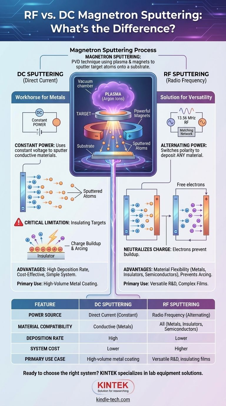
The fundamental difference between RF and DC magnetron sputtering lies in the type of electrical power used and, as a result, the materials they can deposit. DC (Direct Current) sputtering uses a constant voltage to sputter electrically conductive materials, while RF (Radio Frequency) sputtering uses an alternating power source, which enables it to effectively sputter non-conductive, insulating materials as well.
While both are powerful thin-film deposition techniques, the core choice is dictated by your target material. DC sputtering is a fast, cost-effective workhorse for metals, but it fails with insulators. RF sputtering is the more versatile solution, capable of handling any material by using an alternating field to overcome the fatal issue of charge buildup.
The Core Mechanism: What is Magnetron Sputtering?
To understand the difference between DC and RF, we must first understand the foundational process they share.
From Solid Target to Thin Film
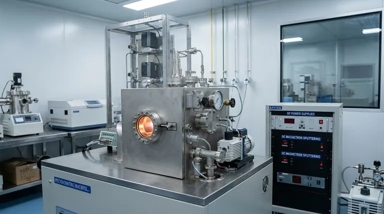
Magnetron sputtering is a Physical Vapor Deposition (PVD) technique. It begins by creating a vacuum in a chamber and introducing an inert gas, typically Argon. A high voltage is applied, which ignites the gas into a plasma—a state of matter containing positive ions and free electrons. These positive Argon ions are then accelerated towards a source material, known as the target, causing atoms to be ejected or "sputtered" from its surface. These sputtered atoms travel through the chamber and deposit onto a substrate, gradually building a uniform thin film.
The Role of the "Magnetron"
The "magnetron" part of the name refers to a critical enhancement. Powerful magnets are placed behind the target. This magnetic field traps electrons from the plasma near the target's surface. These trapped electrons significantly increase the ionization of the Argon gas, creating a much denser plasma. This boosts the sputtering rate, allowing for faster film growth at lower pressures and temperatures. This principle applies to both DC and RF systems.
DC Sputtering: The Workhorse for Metals
Direct Current sputtering is the conceptually simpler of the two methods.
How It Works: A Constant Bombardment
In a DC system, the target is given a constant negative charge, and the chamber acts as the anode (positive). This creates a straightforward electrostatic field that continuously accelerates the positive Argon ions from the plasma toward the target. The result is a steady, high-rate bombardment and a consistent stream of sputtered material.
Key Advantages: Speed and Cost
Because the power supply is simple and the process is direct, DC sputtering offers high deposition rates for conductive materials. The equipment is generally less complex and less expensive than RF systems, making it the go-to choice for high-volume industrial coating of metals like aluminum, copper, and titanium.
The Critical Limitation: Insulating Targets
The strength of DC sputtering is also its fatal weakness. If you attempt to sputter an insulating (dielectric) material like a ceramic or an oxide, positive Argon ions strike the target and their charge has nowhere to go. A positive charge rapidly builds up on the target surface. This "surface charging" repels incoming positive Argon ions, quickly bringing the sputtering process to a halt. In worse cases, this can lead to arcing, which can damage the target and the power supply.
RF Sputtering: The Solution for Versatility
Radio Frequency sputtering was developed specifically to overcome the limitations of the DC method.
How It Works: The Alternating Field
Instead of a constant DC voltage, an RF system uses an AC power source that operates at a high frequency (typically 13.56 MHz). The polarity of the target rapidly switches from negative to positive millions of times per second.
During the negative half-cycle, the target attracts and is bombarded by positive Argon ions, just like in DC sputtering. Crucially, during the brief positive half-cycle, the target attracts a flood of free electrons from the plasma. These electrons instantly neutralize the positive charge that accumulated during the sputtering phase, effectively "resetting" the target surface.
Key Advantage: Material Flexibility
By preventing charge buildup, RF sputtering can reliably deposit any type of material. This includes:
- Insulators: Oxides, nitrides, and ceramics.
- Semiconductors: Such as silicon.
- Conductors: All metals that can be deposited with DC.
This makes RF sputtering an indispensable tool for research and for fabricating advanced devices with complex multi-layer material stacks.
Understanding the Trade-offs
Choosing between RF and DC sputtering involves balancing performance, cost, and material requirements.
Deposition Rate
For a given metallic material, DC sputtering is generally faster than RF sputtering. The alternating cycle of RF means the target is only being sputtered for a portion of the time, slightly reducing overall efficiency compared to the continuous bombardment of a DC system.
System Complexity and Cost
RF systems are inherently more complex. They require an RF power generator and an impedance matching network to efficiently transfer power to the plasma. This makes RF sputtering systems more expensive to purchase and maintain than their DC counterparts.
A Third Option: Pulsed DC Sputtering
A hybrid technique, Pulsed DC, exists to bridge the gap. It uses a DC power source that is turned on and off in very short pulses. This pulsing helps to discharge the target surface before significant arcing can occur. It can be a good compromise for sputtering certain semi-insulating or reactive films, offering better stability than standard DC without the full cost and complexity of RF.
Making the Right Choice for Your Goal
Your decision ultimately comes down to the material you need to deposit and your operational priorities.
- If your primary focus is high-volume, low-cost deposition of metals: DC magnetron sputtering is the optimal choice for its superior speed and economic efficiency.
- If your primary focus is depositing insulating or ceramic materials: RF magnetron sputtering is the required method, as DC is not a viable option.
- If your primary focus is versatility for R&D with a wide range of materials: An RF sputtering system provides the essential flexibility to handle conductors, semiconductors, and insulators alike.
By understanding the fundamental role of the power source, you can confidently select the sputtering technique that directly enables your specific thin-film application.
Summary Table:
| Feature | DC Sputtering | RF Sputtering |
|---|---|---|
| Power Source | Direct Current (Constant) | Radio Frequency (Alternating) |
| Material Compatibility | Conductive Materials (Metals) | All Materials (Metals, Insulators, Semiconductors) |
| Deposition Rate | High | Lower |
| System Cost | Lower | Higher |
| Primary Use Case | High-volume metal coating | Versatile R&D, insulating films |
Ready to choose the right sputtering system for your lab? KINTEK specializes in lab equipment and consumables, serving laboratory needs. Whether you require the high-speed efficiency of DC sputtering for metals or the versatile capabilities of RF sputtering for insulators, our experts can help you select the perfect solution. Contact us today to discuss your thin-film deposition requirements and enhance your research capabilities!
Visual Guide
Related Products
- Microwave Plasma Chemical Vapor Deposition MPCVD Machine System Reactor for Lab and Diamond Growth
- Chemical Vapor Deposition CVD Equipment System Chamber Slide PECVD Tube Furnace with Liquid Gasifier PECVD Machine
- Molybdenum Tungsten Tantalum Special Shape Evaporation Boat
- Hemispherical Bottom Tungsten Molybdenum Evaporation Boat
- Inclined Rotary Plasma Enhanced Chemical Vapor Deposition PECVD Equipment Tube Furnace Machine
People Also Ask
- What is microwave plasma chemical vapor deposition? A Guide to High-Purity Diamond Film Growth
- What are the advantages of a Microwave Plasma CVD reactor for MCD/NCD coatings? Precision Multilayer Diamond Engineering
- How does a microwave plasma reactor facilitate the synthesis of diamond? Master MPCVD with Precision Technology
- What are the primary advantages of the CVD method for growing diamonds? Engineering High-Purity Gems and Components
- Why is argon-rich gas phase chemistry used for UNCD growth? Unlock Precision Nano-Diamond Synthesis