In short, substrate temperature is one of the most critical parameters in sputtering, directly controlling the energy of the atoms as they land on the surface. This single variable profoundly influences nearly every important characteristic of the final thin film, including its density, crystal structure, internal stress, and adhesion to the substrate.
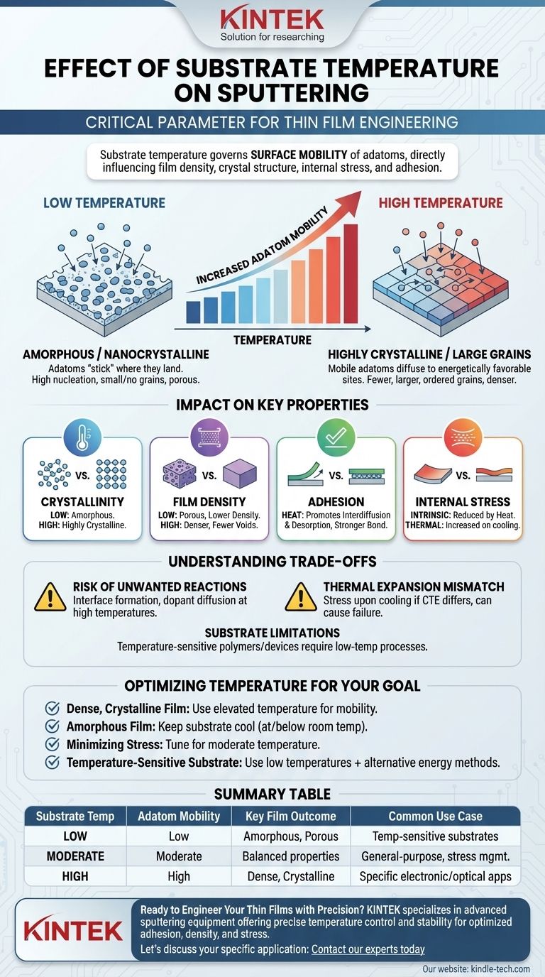
The core principle to understand is this: substrate temperature governs the surface mobility of deposited atoms. By controlling temperature, you are not just heating or cooling the sample; you are dictating how those atoms arrange themselves, which ultimately determines the film's final structure and performance.
The Physics: How Temperature Influences Film Growth
At the atomic scale, the sputtering process is a chaotic arrival of energetic particles. Temperature brings order to this chaos.
Adatom Mobility
When an atom from the sputtering target lands on the substrate, it is called an adatom. This adatom has a certain amount of energy.
Higher substrate temperatures transfer thermal energy to these adatoms. This gives them more energy to move, or diffuse, across the surface before they lose their energy and lock into place.
Nucleation and Grain Growth
Film growth begins with nucleation, where adatoms cluster together to form stable islands. The mobility of these adatoms dictates this process.
At low temperatures, adatoms have little energy and "stick" where they land. This results in a high number of small nucleation sites, leading to a film with very small grains (nanocrystalline) or no ordered structure at all (amorphous).
At high temperatures, mobile adatoms can travel further to find more energetically favorable sites, such as an existing island. This leads to fewer, larger, and more perfectly formed crystalline grains.
Impact on Key Film Properties
Controlling adatom mobility through temperature allows you to directly engineer the final properties of your film.
Crystallinity
Higher temperatures promote the growth of highly ordered, crystalline films with larger grain sizes. This is often desirable for applications requiring specific electronic or optical properties.
Conversely, keeping the substrate cool is a primary method for producing amorphous films, which are valued for their uniformity and lack of grain boundaries.
Film Density
With increased mobility from higher temperatures, adatoms can find and fill microscopic voids and valleys on the surface. This allows them to settle into a more tightly packed arrangement.
The result is a denser, less porous film with fewer defects. Low-temperature depositions often result in more porous films with lower density.
Adhesion
Gently heating the substrate before and during deposition can significantly improve adhesion. This occurs for two reasons: it can desorb contaminants like water from the substrate surface, and it promotes interdiffusion at the film-substrate interface, creating a stronger chemical and mechanical bond.
Internal Stress
Stress is a critical property that can cause films to crack, peel, or deform the substrate. Substrate temperature influences stress in two ways.
First, it affects intrinsic stress, which develops during growth. Higher temperatures often help reduce tensile stress by allowing atoms to arrange in a more relaxed state.
Second, it creates thermal stress upon cooling due to a mismatch in the coefficient of thermal expansion (CTE) between the film and the substrate. This is a critical trade-off to manage.
Understanding the Trade-offs
While heating the substrate is a powerful tool, it is not without its challenges and potential downsides.
Risk of Unwanted Reactions
Elevated temperatures can trigger unwanted chemical reactions between the deposited film and the substrate. This can form an undesirable intermediate layer, altering the properties of the interface.
For doped films, high temperatures can also cause the dopants to diffuse out of the film or into the substrate, ruining the film's intended function.
Thermal Expansion Mismatch
If a film is deposited at a high temperature on a substrate with a different CTE, significant stress will develop as the system cools to room temperature. This can cause catastrophic film failure and must be carefully calculated and managed.
Substrate Limitations
Many important substrates, such as polymers or certain semiconductor devices, are temperature-sensitive and cannot withstand high deposition temperatures. In these cases, you are forced to work within a low-temperature process window, requiring other methods to optimize film properties.
Optimizing Temperature for Your Goal
The "correct" substrate temperature is entirely dependent on the desired outcome for your thin film.
- If your primary focus is a dense, highly crystalline film: Use an elevated substrate temperature to maximize adatom mobility and promote large grain growth.
- If your primary focus is an amorphous film: Keep the substrate at or below room temperature, using active cooling if necessary to remove heat from the sputtering plasma.
- If your primary focus is minimizing film stress: This requires careful tuning, often using a moderate temperature to reduce intrinsic stress without introducing excessive thermal stress upon cooling.
- If your primary focus is depositing on a temperature-sensitive substrate: You must work at low temperatures and may need to use other techniques (like ion beam assistance or substrate biasing) to add energy to the growing film.
Ultimately, mastering substrate temperature control transforms it from a simple variable into a precise tool for engineering thin films to your exact specifications.
Summary Table:
| Substrate Temperature | Adatom Mobility | Key Film Outcome | Common Use Case |
|---|---|---|---|
| Low | Low | Amorphous or nanocrystalline, porous | Temperature-sensitive substrates (polymers) |
| High | High | Dense, highly crystalline, large grains | Applications requiring specific electronic/optical properties |
| Moderate | Moderate | Balanced density and stress, improved adhesion | General-purpose coatings, stress management |
Ready to Engineer Your Thin Films with Precision?
The substrate temperature is just one of the critical parameters in achieving your desired film properties. At KINTEK, we specialize in providing advanced sputtering equipment and consumables that offer precise temperature control and process stability. Whether you are developing highly crystalline films for electronics or depositing on sensitive polymer substrates, our solutions are designed to help you optimize adhesion, density, and stress for superior performance.
Let’s discuss your specific application: Contact our experts today to find the perfect lab equipment for your thin film challenges.
Visual Guide
Related Products
- Spark Plasma Sintering Furnace SPS Furnace
- Vacuum Induction Melting Spinning System Arc Melting Furnace
- Chemical Vapor Deposition CVD Equipment System Chamber Slide PECVD Tube Furnace with Liquid Gasifier PECVD Machine
- Customer Made Versatile CVD Tube Furnace Chemical Vapor Deposition Chamber System Equipment
- Vacuum Cold Mounting Machine for Sample Preparation
People Also Ask
- Why are Spark Plasma Sintering (SPS) furnaces or hot presses utilized in the preparation of Li3PS4 solid electrolytes?
- What are the advantages of CAMI/SPS for W-Cu composite preparation? Reduce cycles from hours to seconds.
- What is the pressure for spark plasma sintering? A Guide to Optimizing SPS Parameters
- What technical advantages does a Spark Plasma Sintering (SPS) furnace offer for LZP ceramics? Enhance Ionic Conductivity
- What are the fundamentals of spark plasma sintering process? Unlock Rapid, High-Performance Material Consolidation


