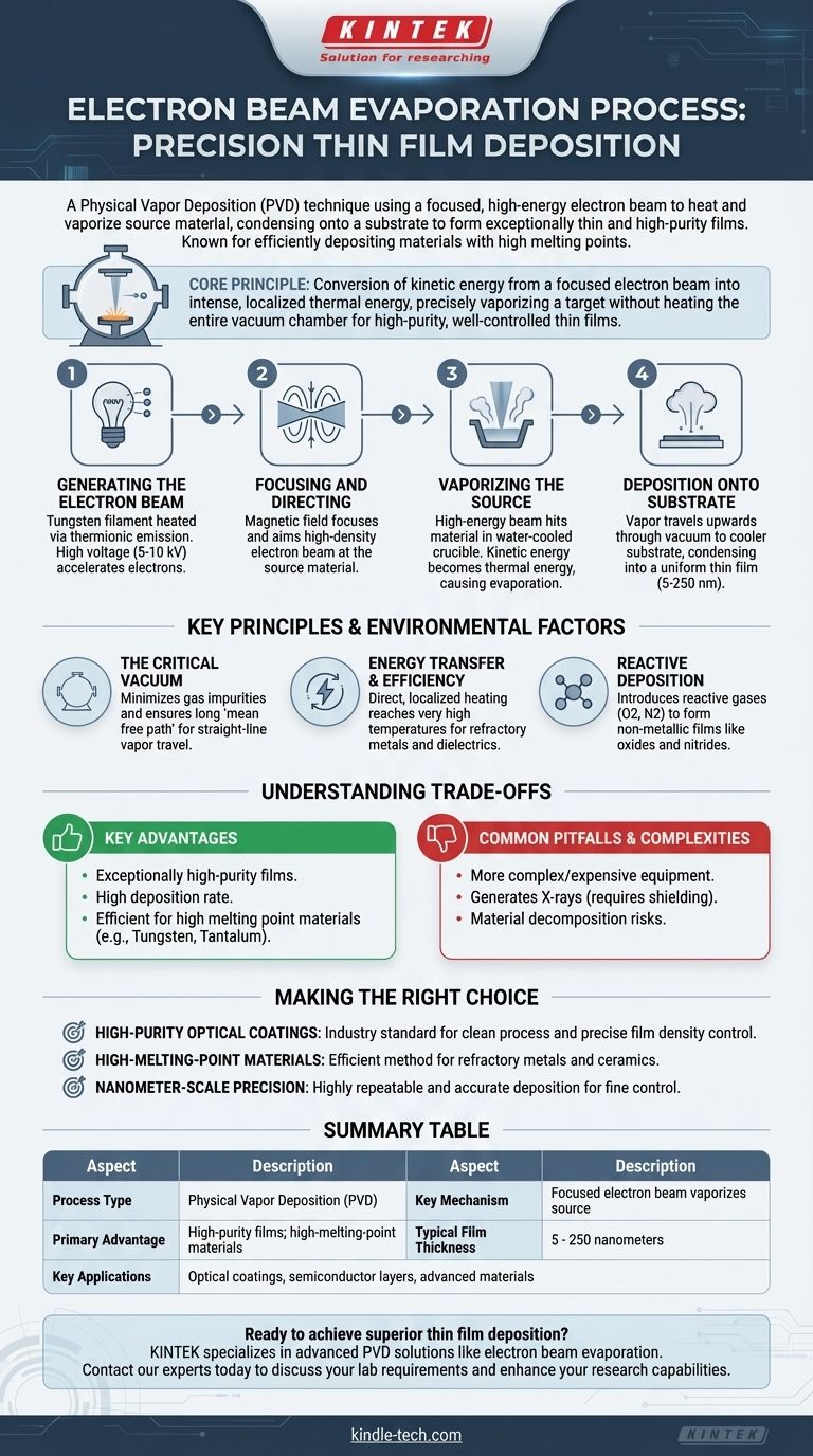
In short, electron beam evaporation is a physical vapor deposition (PVD) technique that uses a focused, high-energy beam of electrons to heat and vaporize a source material inside a vacuum chamber. This vapor then travels and condenses onto a substrate, forming an exceptionally thin and high-purity film. The process is defined by its ability to efficiently deposit materials with very high melting points.
The core principle of electron beam evaporation is the conversion of the kinetic energy from a focused electron beam into intense, localized thermal energy. This allows for the precise vaporization of a target material without heating the entire vacuum chamber, ensuring the creation of highly pure, well-controlled thin films.
The Step-by-Step Process of E-Beam Evaporation
To understand its advantages, it's essential to break down the mechanics of the process. Each step is precisely controlled to achieve a specific outcome in film quality and thickness.
Step 1: Generating the Electron Beam
The process begins with an electron source, typically a tungsten filament. A strong electric current is passed through this filament, heating it to a temperature where it begins to emit electrons via a process called thermionic emission.
A high voltage, often between 5 and 10 kilovolts (kV), is then applied to accelerate these free electrons away from the filament at high speed.
Step 2: Focusing and Directing the Beam
Once accelerated, the stream of electrons is shaped and directed by a magnetic field. This field acts like a lens, focusing the electrons into a narrow, high-density beam aimed at the source material.
This precise control allows the energy to be delivered to a very specific spot on the target.
Step 3: Vaporizing the Source Material
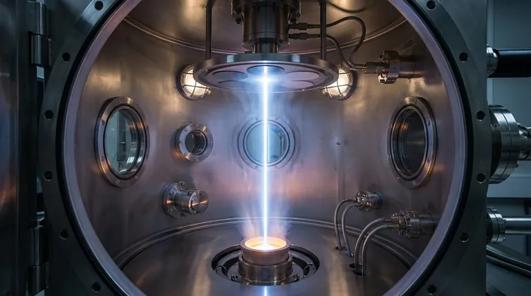
The source material, or evaporant, is held in a water-cooled copper crucible or hearth. When the high-energy electron beam strikes the material, its kinetic energy is instantly converted into intense thermal energy.
This localized heating is extremely efficient, causing the material to rapidly melt and then evaporate (or sublimate, turning directly from solid to gas). The water-cooling of the crucible is critical to prevent the container itself from melting and contaminating the process.
Step 4: Deposition onto the Substrate
The vaporized material travels in a gaseous phase upward through the vacuum chamber. It eventually reaches the much cooler substrate, which is positioned directly above the source.
Upon contact with the cooler surface, the vapor condenses back into a solid state, forming a uniform, thin film. The thickness of this film typically ranges from 5 to 250 nanometers.
Key Principles and Environmental Factors
The effectiveness of electron beam evaporation hinges on a few fundamental principles that differentiate it from other deposition methods.
The Critical Role of the Vacuum
The entire process is conducted within a high-vacuum environment. This is essential for two reasons. First, it minimizes the presence of ambient gas molecules that could react with the vapor and cause impurities in the final film.
Second, the vacuum ensures the vaporized particles can travel in a straight line from the source to the substrate without collision, a concept known as a long "mean free path."
Energy Transfer and Efficiency
The direct energy transfer from electrons to the source material is highly efficient. Unlike simpler thermal evaporation where the entire crucible is heated, e-beam evaporation heats only the material itself.
This allows the process to reach the very high temperatures needed to vaporize refractory metals and dielectric materials that are difficult or impossible to deposit using other methods.
Reactive Deposition
The process can be adapted for more complex materials. By introducing a controlled amount of a reactive gas, such as oxygen or nitrogen, into the chamber during deposition, it's possible to form non-metallic films like oxides and nitrides on the substrate.
Understanding the Trade-offs
Like any advanced technical process, e-beam evaporation has distinct advantages and limitations that make it suitable for specific applications.
Key Advantages
The primary benefit is the ability to create exceptionally high-purity films. The localized heating and vacuum environment prevent contamination from the crucible or atmospheric gases.
Furthermore, it offers a high deposition rate and is one of the only methods capable of efficiently evaporating materials with very high melting points, such as tungsten or tantalum.
Common Pitfalls and Complexities
The equipment required for e-beam evaporation is significantly more complex and expensive than that for thermal evaporation.
The high-energy electron beam can also generate X-rays, which necessitates proper shielding for operator safety. Additionally, some materials may decompose at the high temperatures involved, and stray electrons can sometimes damage the substrate or the growing film.
Making the Right Choice for Your Goal
Selecting a deposition method depends entirely on the requirements for the final film. E-beam evaporation excels in applications where purity and material properties are paramount.
- If your primary focus is high-purity optical coatings: E-beam evaporation is the industry standard due to its clean vacuum process and precise control over film density.
- If you need to deposit high-melting-point metals or ceramics: The intense, localized energy of the electron beam makes it one of the few viable and efficient methods.
- If your application requires precise, nanometer-scale film thickness: The stability and fine control of the electron beam allow for highly repeatable and accurate deposition.
Ultimately, electron beam evaporation is a powerful and versatile tool for engineering material surfaces at the nanoscale, enabling advancements in electronics, optics, and advanced materials.
Summary Table:
| Aspect | Description |
|---|---|
| Process Type | Physical Vapor Deposition (PVD) |
| Key Mechanism | Focused electron beam vaporizes source material |
| Primary Advantage | High-purity films; capable of depositing high-melting-point materials |
| Typical Film Thickness | 5 - 250 nanometers |
| Key Applications | Optical coatings, semiconductor layers, advanced materials |
Ready to achieve superior thin film deposition in your lab?
KINTEK specializes in advanced lab equipment, including solutions for Physical Vapor Deposition (PVD) processes like electron beam evaporation. Whether you are developing optical coatings, semiconductor devices, or advanced materials, our expertise and high-quality equipment can help you achieve the high-purity, precise results you need.
Contact our experts today to discuss how we can support your specific laboratory requirements and enhance your research and development capabilities.
Visual Guide
Related Products
- Electron Beam Evaporation Coating Tungsten Crucible and Molybdenum Crucible for High Temperature Applications
- Electron Beam Evaporation Coating Oxygen-Free Copper Crucible and Evaporation Boat
- Electron Beam Evaporation Coating Gold Plating Tungsten Molybdenum Crucible for Evaporation
- Electron Beam Evaporation Coating Conductive Boron Nitride Crucible BN Crucible
- E Beam Crucibles Electron Gun Beam Crucible for Evaporation
People Also Ask
- What is the current of e-beam evaporation? A Guide to High-Purity Thin Film Deposition
- What is the temperature of e-beam evaporation? Mastering the Two-Zone Thermal Process for Precision Films
- What is e-beam evaporation used for? Precision Coating for Optics, Aerospace & Electronics
- What are the applications of e-beam evaporation? Achieve High-Purity Coatings for Optics & Electronics
- What is the voltage of e-beam evaporation? Achieve Precise Thin-Film Deposition


