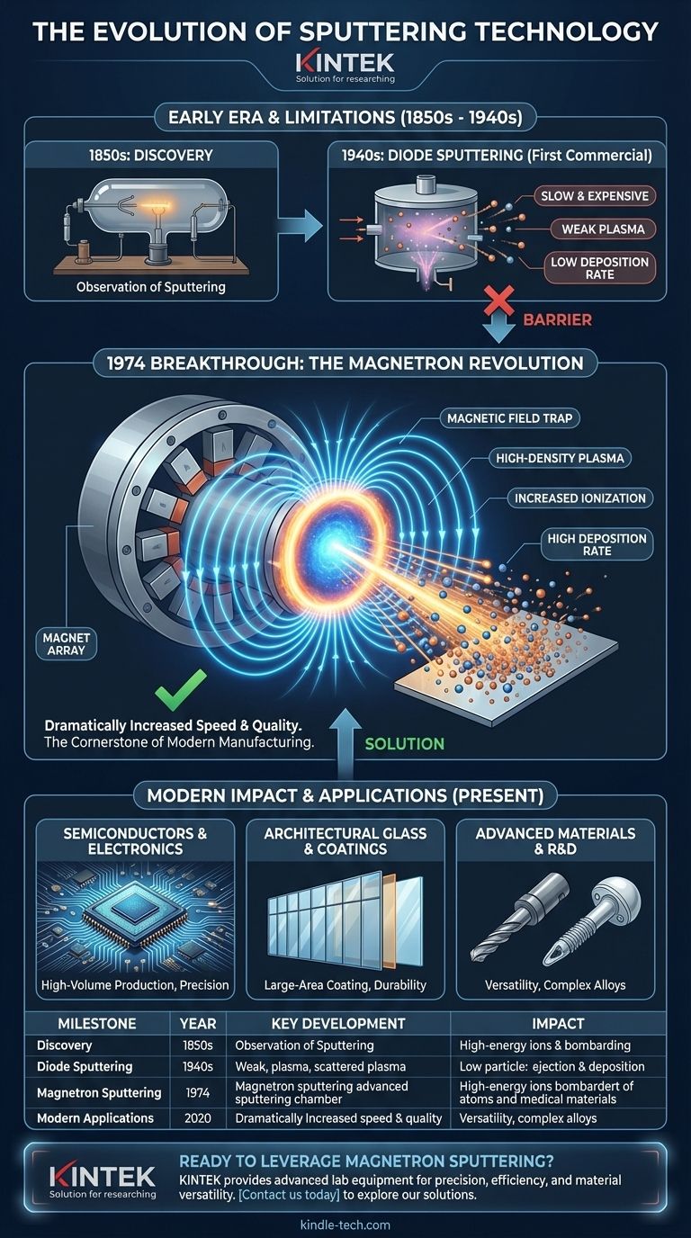
In short, magnetron sputtering was introduced in 1974 as a revolutionary improvement over earlier sputtering techniques. While the basic principle of sputtering had been known since the 1850s, previous methods like diode sputtering were too slow and expensive for widespread industrial use. The 1974 innovation was the addition of a magnetic field, which dramatically increased deposition speed and film quality, transforming sputtering into a cornerstone of modern manufacturing.
The history of magnetron sputtering is not about the invention of a new concept, but about a critical evolution. By using magnets to confine plasma near the target material, it solved the fundamental efficiency problems that had limited sputtering technology for decades, paving the way for its use in everything from semiconductors to architectural glass.
The Problem with Early Sputtering Methods
Sputtering as a physical phenomenon was first observed in the 1850s. The process involves ejecting atoms from a solid target material by bombarding it with energetic ions in a vacuum.
The First Commercial Application: Diode Sputtering
By the 1940s, this phenomenon was harnessed in a process called diode sputtering. It worked, but it was plagued by significant limitations that prevented its broad adoption.
The Core Limitation: Inefficiency
The primary issue with diode sputtering was its extremely low deposition rate. The plasma created to generate the ions was weak and unstable, meaning few ions actually struck the target with enough force to sputter material effectively.
The High-Cost Barrier
This inefficiency directly led to high operational costs and long processing times. For most industrial applications, it was simply not a commercially viable method for producing thin films.
The 1974 Breakthrough: Adding a Magnetic Field
The landscape of thin-film deposition changed completely in 1974 with the introduction of the magnetron. The solution was elegant: place a strong magnetic field on the cathode, directly behind the sputtering target.
How Magnets Changed the Game
This magnetic field acts as a trap for electrons. Instead of escaping to the chamber walls, electrons are forced into a spiral path near the surface of the target material.
Creating a High-Density Plasma
This electron trapping dramatically increases the probability of electrons colliding with and ionizing the inert gas atoms (typically Argon). The result is a dense, stable, and highly concentrated plasma directly in front of the target.
The Result: A Faster, Better Process
This high-density plasma provides a much larger supply of positive ions to bombard the target. This massively increases the sputtering rate—often by an order of magnitude or more—while also allowing the process to run at lower gas pressures, leading to higher purity films.
The Lasting Impact of Magnetron Sputtering
The invention of magnetron sputtering wasn't just an incremental improvement; it unlocked a new level of capability and control in material science and manufacturing.
Unlocking Material Versatility
The process is incredibly flexible and material-independent. It can be used to deposit thin films from a vast range of materials, including pure metals, complex alloys, and even ceramic or insulating compounds.
Enabling Precise and Complex Films
The stability and control offered by magnetron sputtering allow for advanced techniques. Co-sputtering from multiple targets can create custom alloys, while introducing gases like oxygen or nitrogen (reactive sputtering) can form compound films like oxides and nitrides.
Achieving Superior Film Quality
Atoms sputtered via a magnetron process have high kinetic energy. This allows them to form exceptionally dense, uniform, and well-adhered films that penetrate slightly into the substrate surface, improving durability and overall performance.
Common Pitfalls and Considerations
While powerful, magnetron sputtering is a complex process with inherent trade-offs that require expert management.
Target Material Utilization
In a standard planar magnetron, the plasma is confined to a specific "racetrack" zone on the target. This leads to uneven erosion, meaning a significant portion of the expensive target material is often left unused.
Process Control Complexity
The quality of the final film is highly dependent on a careful balance of multiple parameters. Variables like gas pressure, power, temperature, and magnetic field strength must be precisely controlled to achieve repeatable results.
Equipment and Material Costs
The initial investment for magnetron sputtering systems, including high-vacuum chambers, specialized power supplies, and cooling systems, can be substantial. Furthermore, the high-purity target materials required for quality films represent a significant ongoing operational cost.
How This History Informs Modern Applications
Understanding the core innovation—using a magnetic field to increase plasma density and efficiency—is key to appreciating why magnetron sputtering remains essential today.
- If your primary focus is high-volume production: The dramatically increased deposition rates pioneered in 1974 are precisely why this method is used for coating massive surfaces like architectural glass or producing billions of semiconductor chips.
- If your primary focus is advanced material development: The process's versatility, which allows for co-sputtering alloys and reactively sputtering compounds, is the foundation for creating materials with unique optical, electrical, or mechanical properties.
- If your primary focus is surface durability: The high-energy plasma, a direct result of the magnetron design, is what creates the dense, tightly bonded hard coatings essential for protecting cutting tools, medical implants, and automotive components.
Ultimately, the 1974 introduction of the magnetron transformed sputtering from a scientific curiosity into a powerful and indispensable industrial tool that continues to enable technological progress.
Summary Table:
| Milestone | Year | Key Development | Impact |
|---|---|---|---|
| Discovery of Sputtering | 1850s | Observation of atom ejection by ion bombardment | Foundation of the physical phenomenon |
| Diode Sputtering | 1940s | First commercial application | Proved concept but was slow and expensive |
| Magnetron Sputtering | 1974 | Introduction of magnetic field to confine plasma | Dramatically increased deposition rates and film quality |
| Modern Applications | Present | Used in semiconductors, architectural glass, and advanced materials | Cornerstone of high-volume manufacturing and R&D |
Ready to leverage the power of magnetron sputtering in your lab? KINTEK specializes in advanced lab equipment and consumables, including sputtering systems designed for precision, efficiency, and material versatility. Whether you're engaged in semiconductor research, developing durable coatings, or creating complex alloy films, our solutions are tailored to meet your specific laboratory needs. Contact us today to explore how our expertise can enhance your thin-film deposition processes and drive your innovations forward.
Visual Guide
Related Products
- RF PECVD System Radio Frequency Plasma-Enhanced Chemical Vapor Deposition RF PECVD
- Chemical Vapor Deposition CVD Equipment System Chamber Slide PECVD Tube Furnace with Liquid Gasifier PECVD Machine
- Split Chamber CVD Tube Furnace with Vacuum Station Chemical Vapor Deposition System Equipment Machine
- Vacuum Hot Press Furnace Heated Vacuum Press Machine Tube Furnace
- 1200℃ Controlled Atmosphere Furnace Nitrogen Inert Atmosphere Furnace
People Also Ask
- What is plasma enhanced chemical vapor deposition PECVD equipment? A Guide to Low-Temperature Thin Film Deposition
- What is the plasma CVD process? Achieve Low-Temperature Thin Film Deposition
- What is plasma activated chemical vapour deposition method? A Low-Temperature Solution for Advanced Coatings
- How are PECVD and CVD different? A Guide to Choosing the Right Thin-Film Deposition Process
- Why does PECVD commonly use RF power input? For Precise Low-Temperature Thin Film Deposition