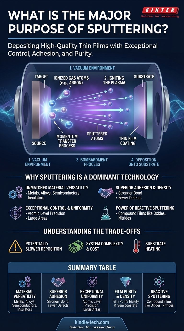
At its core, the major purpose of sputtering is to deposit a high-quality, extremely thin film of a specific material onto a surface. It is a physical vapor deposition (PVD) method where atoms are physically ejected from a source material, called a target, and then land on a substrate to form a uniform coating. This process is essential for manufacturing countless high-technology products, from microchips to architectural glass.
The true value of sputtering is not just its ability to create a thin film, but its power to do so with exceptional control, for nearly any material, resulting in films with superior adhesion, purity, and uniformity that are difficult to achieve with other methods.
How Sputtering Works: From Plasma to Film
Sputtering is fundamentally a momentum transfer process. Think of it as a microscopic-scale sandblaster, but instead of sand, it uses ionized gas atoms to precisely chip away at a source material.
The Vacuum Environment
First, a substrate (the object to be coated) and a target (the source material) are placed inside a vacuum chamber. The chamber is pumped down to remove air and other contaminants that could compromise the purity of the film.
Igniting the Plasma
An inert gas, most commonly argon, is then introduced into the chamber at low pressure. A high voltage is applied to the target, causing it to become a negatively charged cathode. This electrical field energizes the gas, stripping electrons from the argon atoms and creating a glowing, ionized gas known as a plasma.
The Bombardment Process
The positively charged argon ions within the plasma are now forcefully accelerated toward the negatively charged target. They collide with the target surface with significant energy.
This high-energy impact is powerful enough to knock out, or "sputter," individual atoms or molecules from the target material.
Deposition onto the Substrate
These ejected target particles travel in a straight line through the vacuum chamber. When they encounter the substrate, they land on its surface, gradually building up layer by layer to form a dense, uniform, and extremely thin film.
Why Sputtering Is a Dominant Technology
Engineers and scientists choose sputtering when the quality and properties of the deposited film are critical. The process offers several distinct advantages over simpler techniques like thermal evaporation.
Unmatched Material Versatility
Sputtering can deposit virtually any material. This includes high-melting-point metals, complex alloys, semiconductors, and even insulating compounds and mixtures. Because the target material is physically ejected rather than boiled, its melting point is irrelevant.
Superior Film Adhesion and Density
Sputtered atoms arrive at the substrate with high kinetic energy. This energy helps them form a much stronger bond with the substrate surface, resulting in excellent adhesion. This energy also ensures the atoms pack together tightly, creating a very dense film with fewer defects or pinholes.
Exceptional Control and Uniformity
The process is highly controllable and reproducible. By precisely managing the gas pressure, voltage, and time, operators can control the film's thickness down to the atomic level. This control makes it possible to produce highly uniform films over very large surface areas, a key requirement for mass production.
The Power of Reactive Sputtering
A powerful variation involves adding a reactive gas, like oxygen or nitrogen, to the chamber along with the argon. By sputtering a metal target (e.g., titanium) in the presence of nitrogen, one can deposit a compound film (titanium nitride) on the substrate. This greatly expands the range of materials that can be created.
Understanding the Trade-offs
While powerful, sputtering is not the universal solution for every coating application. It's important to recognize its limitations.
Potentially Slower Deposition Rates
Compared to some high-rate thermal evaporation processes, sputtering can be a slower method for building up thick films. The rate of deposition is limited by how efficiently ions can eject material from the target.
System Complexity and Cost
Sputtering systems require a vacuum chamber, high-voltage power supplies, and precise gas flow controllers. This equipment is inherently more complex and expensive than simpler deposition techniques.
Substrate Heating
The constant bombardment of high-energy particles (sputtered atoms and plasma ions) can transfer significant heat to the substrate. This can be a problem when coating temperature-sensitive materials like certain plastics or biological samples, often requiring dedicated substrate cooling.
Making the Right Choice for Your Application
The decision to use sputtering hinges on the specific requirements of the final product.
- If your primary focus is depositing complex alloys or high-melting-point materials: Sputtering is the superior choice because it does not require melting the source material.
- If your primary focus is achieving the strongest possible film adhesion and durability: Sputtering's high-energy deposition process creates an exceptionally robust bond to the substrate.
- If your primary focus is coating a large area with a highly uniform, pure, and reproducible film: Sputtering offers the process control necessary for high-volume, high-precision manufacturing.
- If your primary focus is creating specific compound films like oxides or nitrides: Reactive sputtering provides a highly controlled method to form these coatings directly during deposition.
Ultimately, sputtering is the definitive technology for applications that demand high-performance thin films with precisely engineered properties.
Summary Table:
| Key Advantage | Description |
|---|---|
| Material Versatility | Deposits metals, alloys, semiconductors, and insulating compounds. |
| Superior Adhesion | High-energy particles create a strong, durable bond to the substrate. |
| Exceptional Uniformity | Precise control enables highly uniform coatings over large areas. |
| Film Purity & Density | Vacuum environment and momentum transfer result in dense, pure films. |
| Reactive Sputtering | Creates compound films (e.g., oxides, nitrides) by adding reactive gases. |
Need a high-performance thin film for your product?
KINTEK specializes in advanced sputtering solutions and lab equipment for R&D and manufacturing. Whether you are developing microchips, coated glass, or next-generation semiconductors, our expertise ensures you achieve the superior adhesion, purity, and uniformity your project demands.
Contact our experts today to discuss how our sputtering systems and consumables can enhance your laboratory's capabilities and bring your high-technology products to market.
Visual Guide
Related Products
- Spark Plasma Sintering Furnace SPS Furnace
- Vacuum Induction Melting Spinning System Arc Melting Furnace
- Chemical Vapor Deposition CVD Equipment System Chamber Slide PECVD Tube Furnace with Liquid Gasifier PECVD Machine
- Customer Made Versatile CVD Tube Furnace Chemical Vapor Deposition Chamber System Equipment
People Also Ask
- What is the theory of spark plasma sintering? A Guide to Rapid, Low-Temperature Densification
- What is the difference between spark plasma sintering and flash sintering? A Guide to Advanced Sintering Methods
- What is the process fundamentals of spark plasma sintering? Achieve Rapid, High-Density Material Consolidation
- What is the pressure for spark plasma sintering? A Guide to Optimizing SPS Parameters
- What are the advantages of CAMI/SPS for W-Cu composite preparation? Reduce cycles from hours to seconds.


