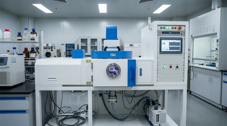
At its core, Physical Vapor Deposition (PVD) is a family of processes used to create high-purity, high-performance thin films and coatings, including those at the nanoscale. In a high-vacuum environment, a solid source material is converted into a vapor through physical means—such as intense heating or ion bombardment. This vapor then travels across the vacuum chamber and condenses onto a target surface (the substrate), building up a film atom by atom.
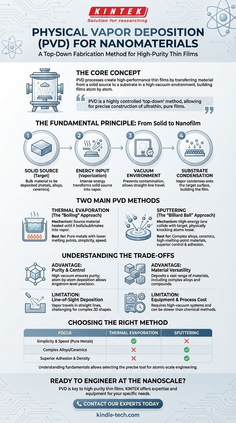
Physical Vapor Deposition is best understood as a highly controlled "top-down" fabrication method. It physically transfers material from a solid source to a substrate in a vacuum, allowing for the precise construction of ultrathin, pure films with specific nanoscale properties.
The Fundamental Principle: From Solid to Nanofilm
PVD processes operate on a shared set of principles, regardless of the specific technique. Understanding this foundation is key to appreciating how nanomaterials are synthesized with such precision.
The Vacuum Environment
Every PVD process takes place in a high-vacuum chamber. This is critical because removing air and other gases prevents the source material vapor from reacting with contaminants, ensuring the purity of the final film. The vacuum also allows atoms to travel in a straight line from the source to the substrate.
The Source Material (Target)
This is the bulk material you intend to deposit. It can be a pure metal, a complex alloy, or a ceramic. The goal of the PVD process is to liberate individual atoms or small clusters of atoms from this target.
The Energy Input
Energy is required to transform the solid source material into a vapor. The type of energy used is the primary distinction between the two main PVD methods. This energy must be sufficient to overcome the atomic bonds holding the solid target together.
The Substrate and Condensation
The substrate is the object onto which the film is deposited. As the vaporized atoms from the source material reach the cooler substrate, they lose their energy and condense, sticking to the surface and building the desired nanostructure or thin film layer by layer.
A Closer Look at the Two Main PVD Methods
While both methods follow the same basic principle, how they generate the vaporized material dictates their advantages and applications. The reference correctly identifies the two dominant PVD techniques.
Thermal Evaporation: The 'Boiling' Approach
In thermal evaporation, the source material is heated in the vacuum chamber until it reaches a temperature where it begins to boil or sublimate directly into a gaseous state.
This method is analogous to boiling water to create steam. A resistive heater or an electron beam provides the intense heat needed to vaporize the solid material, which then coats the substrate.
Sputtering: The 'Billiard Ball' Approach
Sputtering uses momentum transfer instead of heat. Inside the vacuum chamber, a high-voltage electric field energizes a heavy, inert gas (like Argon), creating a plasma.
These high-energy ions are accelerated toward the source material (the target). When they collide, they physically knock atoms loose from the target's surface, a process akin to a cue ball breaking a rack of billiard balls. These ejected atoms then travel to the substrate and form the film.
Understanding the Trade-offs of PVD
PVD is a powerful tool for nanomaterial synthesis, but it is essential to understand its advantages and limitations.
Advantage: Purity and Control
The vacuum environment ensures extremely high purity, as contaminants are minimized. Because deposition occurs atom-by-atom, engineers can control film thickness with Angstrom-level precision (an Angstrom is one-tenth of a nanometer).
Advantage: Material Versatility
PVD can deposit a vast range of materials, including metals, alloys, ceramics, and compounds that are difficult or impossible to process with other methods. Sputtering, in particular, excels at depositing complex alloys without altering their composition.
Limitation: Line-of-Sight Deposition
PVD is a directional process. The vaporized material travels in a straight line from the source to the substrate. This makes it challenging to uniformly coat complex, three-dimensional shapes with intricate geometries or undercuts.
Limitation: Equipment and Process Cost
PVD systems require expensive high-vacuum chambers, sophisticated power supplies, and control systems. The process can also be relatively slow compared to chemical deposition methods, increasing operational costs for large-scale production.
Choosing the Right PVD Method
Selecting the appropriate PVD technique depends entirely on the material being deposited and the desired properties of the final film.
- If your primary focus is simplicity and speed for pure metals with lower melting points: Thermal Evaporation is often the most direct and cost-effective choice.
- If your primary focus is depositing complex alloys, ceramics, or high-melting-point materials: Sputtering offers superior control over composition and works with a much wider range of source materials.
- If your primary focus is creating dense films with strong adhesion to the substrate: Sputtering generally produces films that adhere better and are more densely packed than those from thermal evaporation.
Understanding these fundamental mechanisms allows you to select the precise tool needed to engineer materials at the atomic scale.
Summary Table:
| PVD Method | Key Mechanism | Best For | Key Advantage |
|---|---|---|---|
| Thermal Evaporation | Heating source material to vaporize (boil/sublimate) | Pure metals with lower melting points | Simplicity and speed |
| Sputtering | Ion bombardment to knock atoms off a target | Complex alloys, ceramics, high-melting-point materials | Superior control over film composition and adhesion |
Ready to Engineer at the Nanoscale?
PVD is the key to creating high-purity, high-performance thin films for your most demanding applications. Whether you need the simplicity of thermal evaporation or the advanced capabilities of sputtering, KINTEK has the expertise and equipment to meet your laboratory's specific needs.
Contact our experts today to discuss how our PVD solutions can enhance your research and development. Let KINTEK, your partner in advanced lab equipment, help you achieve atomic-level precision.
Visual Guide
Related Products
- Chemical Vapor Deposition CVD Equipment System Chamber Slide PECVD Tube Furnace with Liquid Gasifier PECVD Machine
- RF PECVD System Radio Frequency Plasma-Enhanced Chemical Vapor Deposition RF PECVD
- 915MHz MPCVD Diamond Machine Microwave Plasma Chemical Vapor Deposition System Reactor
- HFCVD Machine System Equipment for Drawing Die Nano-Diamond Coating
- Microwave Plasma Chemical Vapor Deposition MPCVD Machine System Reactor for Lab and Diamond Growth
People Also Ask
- Why is Chemical Vapor Deposition (CVD) equipment uniquely suited for constructing hierarchical superhydrophobic structures?
- What types of substrates are used in CVD to facilitate graphene films? Optimize Graphene Growth with the Right Catalyst
- What is plasma enhanced chemical vapor deposition PECVD equipment? A Guide to Low-Temperature Thin Film Deposition
- How expensive is chemical vapor deposition? Understanding the True Cost of High-Performance Coating
- What are the advantages of chemical vapor deposition? Achieve Superior Thin Films for Your Lab


