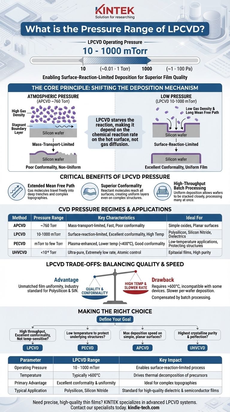
In semiconductor manufacturing, Low-Pressure Chemical Vapor Deposition (LPCVD) operates within a specific vacuum range to achieve its signature film quality. The typical operating pressure for an LPCVD process falls between 10 and 1000 mTorr (millitorr), which is equivalent to approximately 0.01 to 1 Torr or 1 to 100 Pascals (Pa).
The core principle of LPCVD is not simply about reducing pressure, but about using that reduction to shift the deposition from being limited by gas transport to being limited by the surface reaction rate. This fundamental shift is what enables the high-quality, uniform, and conformal films that are essential for modern microelectronics.
Why This Pressure Range is Critical for LPCVD
The choice to operate in this low-pressure regime is a deliberate engineering decision designed to control the physics of the deposition process. It directly influences film uniformity, the ability to coat complex surfaces, and process throughput.
Moving from Diffusion to Surface-Reaction Control
At atmospheric pressure (~760,000 mTorr), the density of gas molecules is very high. The rate at which precursor gases reach a wafer's surface is limited by how quickly they can diffuse through a stagnant boundary layer of gas. This is a mass-transport-limited or diffusion-limited process, which is inherently non-uniform.
By dramatically lowering the pressure into the LPCVD range, we starve the reaction of precursor gas. The process is no longer limited by how fast the gas gets to the surface, but by the rate at which the chemical reaction can occur on the hot surface itself. This is a surface-reaction-limited process.
The Impact of Mean Free Path
Lowering the pressure significantly increases the mean free path—the average distance a gas molecule travels before colliding with another.
In the LPCVD pressure range, the mean free path becomes much longer than the critical dimensions of the features on a wafer. This allows gas molecules to travel freely into deep trenches and complex topographies before reacting.
Achieving Superior Film Conformality
This extended mean free path is the direct cause of LPCVD's hallmark feature: excellent conformality. Because reactant molecules can easily reach all exposed surfaces before reacting, the resulting film deposits in a uniform layer that perfectly conforms to the underlying topography.
Enabling High-Throughput Batch Processing
A surface-reaction-limited process is primarily dependent on temperature, which can be controlled with high precision across a large furnace tube.
This allows wafers to be stacked vertically in "boats" with minimal spacing. Since the deposition rate is uniform everywhere, every wafer in the batch—and every point on each wafer—receives a nearly identical film, enabling high throughput with exceptional uniformity.
Comparing Pressure Regimes: LPCVD vs. Other Methods
The LPCVD pressure range exists within a spectrum of CVD technologies, each optimized for different outcomes.
Atmospheric Pressure CVD (APCVD)
Operating at ambient pressure (~760 Torr), APCVD offers very high deposition rates. However, its mass-transport-limited nature results in poor conformality and makes it suitable only for less demanding applications like simple oxide depositions on planar surfaces.
Plasma-Enhanced CVD (PECVD)
PECVD often operates in a similar pressure range to LPCVD (mTorr to a few Torr). The key difference is its use of a plasma to decompose precursor gases, allowing for deposition at much lower temperatures (typically < 400°C). Pressure is still a factor, but plasma power is the dominant control for the reaction.
Ultra-High Vacuum CVD (UHVCVD)
Operating at pressures below 10⁻⁶ Torr, UHVCVD is used for creating extremely pure, defect-free epitaxial films. The ultra-high vacuum minimizes contamination and allows for precise atomic-level control, but at the cost of exceptionally low deposition rates and throughput.
Understanding the LPCVD Trade-offs
While powerful, the LPCVD pressure and temperature regime comes with inherent compromises.
The Advantage: Unmatched Quality at Scale
The primary benefit is achieving excellent film uniformity and conformality across large batches of wafers simultaneously. For materials like polysilicon and silicon nitride, it is the industry standard for this reason.
The Drawback: High Temperature Requirement
Because LPCVD relies solely on thermal energy to drive the reaction, it requires very high temperatures (e.g., >600°C for polysilicon, >750°C for silicon nitride). This makes it incompatible with devices that already have low-melting-point materials, such as aluminum metallization.
The Consequence: Slower Per-Wafer Deposition
The deposition rates in LPCVD are inherently slower than in APCVD. The process trades raw deposition speed for film quality, compensating for the slower rate by processing many wafers in a single run.
Making the Right Choice for Your Goal
Selecting a deposition method requires matching the process parameters to the desired film properties and device constraints.
- If your primary focus is high throughput and excellent conformality on non-temperature-sensitive devices: LPCVD is the ideal choice for its ability to deliver uniform films in a large-batch process.
- If your primary focus is depositing films at low temperatures to protect underlying structures: PECVD is the necessary alternative, as its plasma allows for high-quality films without high thermal budgets.
- If your primary focus is maximum deposition speed on simple, planar surfaces: APCVD provides the highest throughput when film conformality and uniformity are not primary concerns.
- If your primary focus is achieving the highest possible crystalline purity and perfection: UHVCVD is required for demanding applications like epitaxial growth, despite its very low speed.
Ultimately, the pressure within a CVD reactor is a fundamental parameter that governs the physics of deposition, directly defining the trade-offs between film quality, throughput, and process temperature.
Summary Table:
| Parameter | LPCVD Range | Key Impact |
|---|---|---|
| Operating Pressure | 10 - 1000 mTorr | Enables surface-reaction-limited process |
| Temperature | Typically >600°C | Drives thermal decomposition of precursors |
| Primary Advantage | Excellent conformality & uniformity | Ideal for complex topographies |
| Typical Application | Polysilicon, Silicon Nitride | Standard for high-quality dielectric & semiconductor films |
Need precise, high-quality thin films for your semiconductor or research applications? KINTEK specializes in advanced lab equipment and consumables, including LPCVD systems designed to deliver the uniform, conformal coatings essential for modern microelectronics. Our expertise ensures your laboratory achieves reliable, repeatable results. Contact our specialists today to discuss how our solutions can enhance your deposition processes and meet your specific research or production goals.
Visual Guide
Related Products
- Inclined Rotary Plasma Enhanced Chemical Vapor Deposition PECVD Equipment Tube Furnace Machine
- Inclined Rotary Plasma Enhanced Chemical Vapor Deposition PECVD Equipment Tube Furnace Machine
- Chemical Vapor Deposition CVD Equipment System Chamber Slide PECVD Tube Furnace with Liquid Gasifier PECVD Machine
- Laboratory CVD Boron Doped Diamond Materials
- Microwave Plasma Chemical Vapor Deposition MPCVD Machine System Reactor for Lab and Diamond Growth
People Also Ask
- How does plasma enhance CVD? Unlock Low-Temperature, High-Quality Film Deposition
- How does the PECVD function enhance thin-film properties? Achieve Superior Chemical Stability & Durability
- What is the necessity of depositing a silicon nitride (SiNx) thin film using PECVD? Optimize QSSPC Lifetime Measurement
- What are the core advantages of PE-CVD in OLED encapsulation? Protect Sensitive Layers with Low-Temp Film Deposition
- What is the core value of PECVD compared to CVD? Discover the Low-Temperature Advantage for Thin-Film Coating


