At its core, chemical vapor deposition (CVD) is a sophisticated process for creating high-performance solid coatings by reacting specific gases on a surface. A component is placed in a reaction chamber and exposed to volatile precursor gases, which are then energized, typically by heat or plasma. This energy triggers a chemical reaction, causing a new, solid material to form and bond directly onto the component's surface, building a thin film layer by layer.
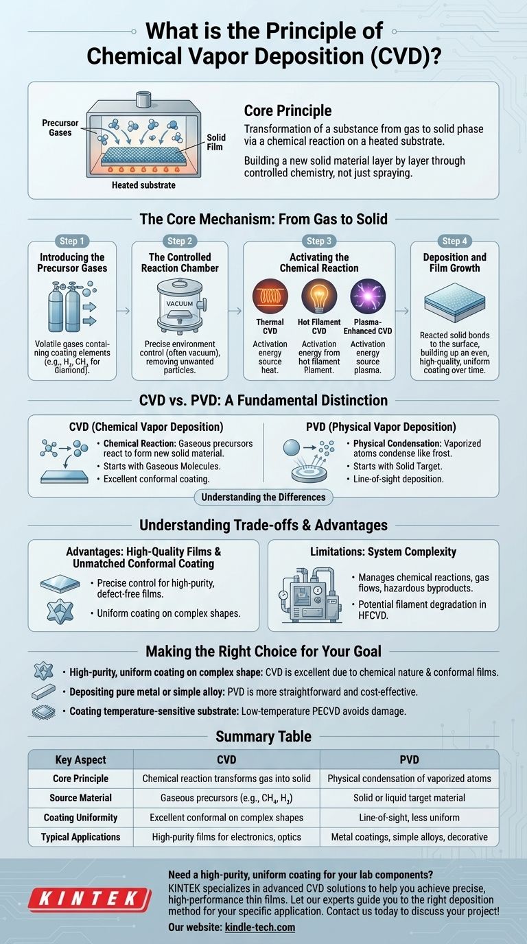
The essential principle of CVD is the transformation of a substance from a gas phase to a solid phase via a chemical reaction on a heated substrate. It isn't simply spraying a material; it's about constructing a new solid material directly on the target surface through controlled chemistry.
The Core Mechanism: From Gas to Solid
To understand CVD, it's best to break the process down into its fundamental stages. Each step is precisely controlled to achieve a film with the desired thickness, composition, and quality.
Introducing the Precursor Gases
The process begins with one or more volatile chemical gases, known as precursors. These gases contain the elements required for the final coating. For example, in diamond film deposition, hydrogen (H₂) and methane (CH₄) are common precursors.
The Controlled Reaction Chamber
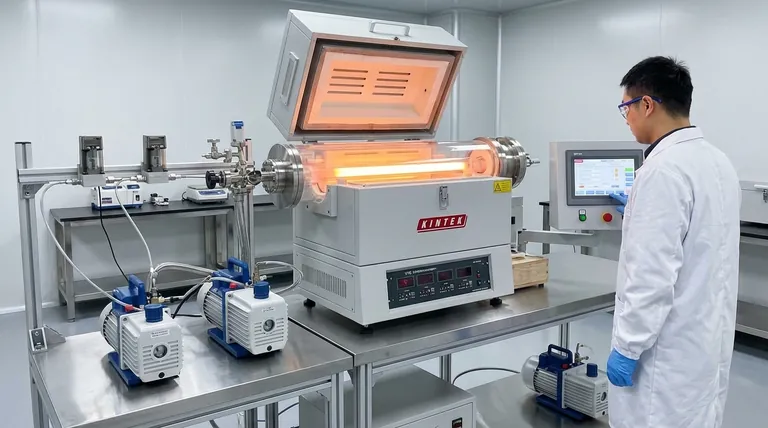
The component to be coated, called the substrate, is placed inside a sealed chamber. This chamber allows for precise control of the environment, often operating under a vacuum to remove unwanted particles and help draw the precursor gases toward the substrate.
Activating the Chemical Reaction
The precursor gases do not react on their own. They require an external energy source to initiate the decomposition and chemical reactions that form the solid film. This is the key activation step.
Common activation methods include:
- Thermal CVD: The substrate is heated to a high temperature, providing the thermal energy needed for the reaction to occur on its surface.
- Hot Filament CVD (HFCVD): A filament made of a refractory metal (like tungsten) is heated to extremely high temperatures (over 2000 K). The precursor gases break down as they pass over this hot filament.
- Plasma-Enhanced CVD (PECVD): Microwaves or other energy sources are used to generate a plasma, an ionized gas containing highly reactive species. This plasma provides the energy to break down the precursors, often allowing the process to run at much lower temperatures.
Deposition and Film Growth
Once the precursor gases react, the resulting solid material bonds to the substrate's surface. This process continues over time, allowing the thin film to build up evenly across the entire exposed surface of the component, creating a high-quality, uniform coating.
CVD vs. PVD: A Fundamental Distinction
It is critical to distinguish chemical vapor deposition (CVD) from its counterpart, physical vapor deposition (PVD). Though both create thin films, their underlying principles are entirely different.
Chemical Reaction vs. Physical Condensation
The defining feature of CVD is the chemical reaction that occurs at the substrate. Gaseous molecules react to form a new, stable solid material that constitutes the film.
In contrast, PVD is a physical process. A solid or liquid source material is vaporized (by heating or sputtering), and the resulting atoms are transported through a vacuum to simply condense on the substrate, like water vapor forming frost on a cold window.
The Nature of the Source Material
CVD starts with gaseous molecules (precursors) that are chemically transformed. PVD starts with a solid target that is physically converted into a vapor of atoms and then deposited without a chemical reaction.
Understanding the Trade-offs and Advantages
CVD is a powerful technique, but its selection depends on understanding its unique benefits and potential complexities.
The Advantage of High-Quality Films
CVD allows for precise control over the chemical reactions, enabling the growth of high-purity, high-performance films that are often free of defects. This level of control is essential for applications in electronics and optics.
Unmatched Conformal Coating
Because the process relies on a gas that can flow into every nook and cranny of a component, CVD provides an exceptionally uniform or "conformal" coating, even on complex, three-dimensional shapes.
System Complexity and Limitations
The primary trade-off is complexity. CVD systems must manage chemical reactions, precursor gas flows, and potentially hazardous byproducts. Additionally, some methods have limitations; for instance, the filaments in HFCVD can degrade over time, affecting process stability.
Making the Right Choice for Your Goal
Selecting the right deposition method depends entirely on the material you are depositing and the properties you need to achieve in the final product.
- If your primary focus is a high-purity, uniform coating on a complex shape: CVD is an excellent choice due to its chemical nature and ability to deliver conformal films.
- If your primary focus is depositing a pure metal or a simple alloy: PVD is often a more straightforward and cost-effective physical process, as no complex reactions are required.
- If your primary focus is coating a temperature-sensitive substrate: A low-temperature variant like Plasma-Enhanced CVD (PECVD) may be necessary to avoid damaging the underlying component.
Ultimately, chemical vapor deposition offers a remarkable ability to construct advanced materials directly on a surface through the power of controlled chemistry.
Summary Table:
| Key Aspect | CVD (Chemical Vapor Deposition) | PVD (Physical Vapor Deposition) |
|---|---|---|
| Core Principle | Chemical reaction transforms gas into solid on the substrate | Physical condensation of vaporized atoms onto the substrate |
| Source Material | Gaseous precursors (e.g., CH₄, H₂) | Solid or liquid target material |
| Coating Uniformity | Excellent conformal coating on complex shapes | Line-of-sight deposition, less uniform on complex geometries |
| Typical Applications | High-purity films for electronics, optics, wear resistance | Metal coatings, simple alloys, decorative finishes |
Need a high-purity, uniform coating for your lab components? KINTEK specializes in lab equipment and consumables, providing advanced CVD solutions to help you achieve precise, high-performance thin films for your research or production needs. Let our experts guide you to the right deposition method for your specific application. Contact us today to discuss your project!
Visual Guide
Related Products
- CVD Diamond Dressing Tools for Precision Applications
- Multi Heating Zones CVD Tube Furnace Machine Chemical Vapor Deposition Chamber System Equipment
- CVD Diamond Domes for Industrial and Scientific Applications
- CVD Diamond for Thermal Management Applications
- Chemical Vapor Deposition CVD Equipment System Chamber Slide PECVD Tube Furnace with Liquid Gasifier PECVD Machine
People Also Ask
- How do you identify a CVD diamond? The Definitive Guide to Lab-Grown Diamond Verification
- What is chemical vapor deposition of diamond? Grow High-Purity Diamonds Atom-by-Atom
- What are the disadvantages of CVD diamonds? Understanding the trade-offs for your purchase.
- What are the raw materials for CVD diamonds? A seed, a gas, and the science of crystal growth.
- How long does it take to make synthetic diamonds? Discover the 6-8 Week Science Behind Lab-Grown Gems


