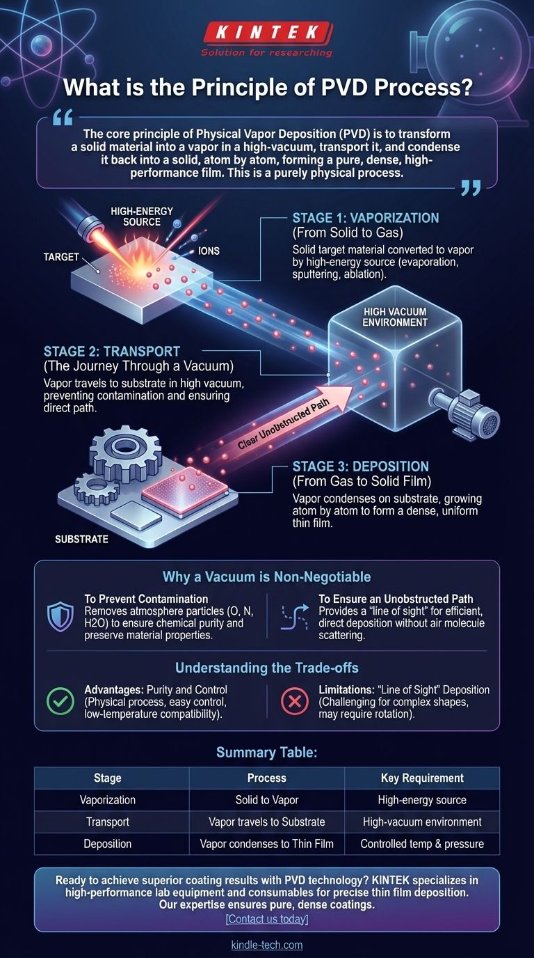
The core principle of Physical Vapor Deposition (PVD) is to transform a solid material into a vapor within a high-vacuum environment, transport that vapor to a substrate, and then condense it back into a solid state to form a thin, high-performance coating. This entire process is purely physical, involving no chemical reactions. The new layer is built atom by atom, resulting in an exceptionally pure and dense film.
PVD is fundamentally a three-step physical transformation: a source material is vaporized in a vacuum, the vapor travels to the object's surface, and it condenses to form a thin film. The vacuum is the critical element that enables this high-purity, controlled deposition.
The Three Foundational Stages of PVD
To understand the PVD process, it is best to break it down into its three distinct and sequential stages. Every PVD application, regardless of the specific technique, follows this fundamental path.
Stage 1: Vaporization (From Solid to Gas)
The process begins with a solid source material, known as the target. This target contains the exact material that will form the final coating.
This solid material must be converted into a gaseous vapor. This is achieved by bombarding it with a high-energy source inside the vacuum chamber. Common methods include high-temperature evaporation, bombardment with high-energy ions (sputtering), or ablation with a laser or electron beam.
Stage 2: Transport (The Journey Through a Vacuum)
Once vaporized, the atoms or molecules of the coating material travel from the target toward the substrate (the object being coated).
This transport phase must occur in a high vacuum. This controlled environment is essential for the integrity of the process, ensuring the vapor particles have a clear, unobstructed path to the substrate.
Stage 3: Deposition (From Gas to Solid Film)
Upon reaching the substrate, which is typically at a lower temperature, the vaporized material condenses. It transitions back into a solid state, forming a thin, tightly bonded film on the substrate's surface.
This film grows atom by atom, which results in a very dense and uniform coating structure. The final thickness can be controlled with extreme precision, often measuring only a few microns or even nanometers.
Why a Vacuum is Non-Negotiable
The use of a high-vacuum environment is not an incidental detail; it is the defining characteristic of PVD and is essential for two primary reasons.
To Prevent Contamination
Normal atmosphere is filled with particles like oxygen, nitrogen, and water vapor that can react with the coating material. A vacuum removes these contaminants.
This ensures the deposited film is chemically pure and consists only of the intended source material, preserving its desired properties like hardness, color, or lubricity.
To Ensure an Unobstructed Path
At atmospheric pressure, the vaporized coating atoms would constantly collide with air molecules, scattering them and preventing them from ever reaching the substrate in a controlled way.
The vacuum provides a clear "line of sight" path from the target to the substrate. This allows for the efficient and direct deposition required to form a high-quality film.
Understanding the Trade-offs
Like any technical process, PVD has inherent strengths and limitations that stem directly from its physical principles. Understanding these is key to its proper application.
The Advantage: Purity and Control
Because PVD is a purely physical process with no chemical reactions, the composition of the final coating is extremely easy to control and predict. It is simply the source material.
Furthermore, many PVD processes run at relatively low temperatures compared to chemical methods (like Chemical Vapor Deposition), making PVD suitable for coating materials that cannot withstand high heat.
The Limitation: "Line of Sight" Deposition
The same "line of sight" principle that ensures efficient transport also creates a primary limitation. PVD is best at coating surfaces that are directly visible from the source material target.
Coating complex, non-planar shapes with deep grooves or internal cavities can be challenging. Parts often require complex rotation and manipulation during the process to achieve uniform coverage across all surfaces.
Making the Right Choice for Your Goal
By understanding the fundamental principle of PVD, you can determine when it is the correct engineering choice for your application.
- If your primary focus is creating a high-purity, dense coating: PVD is ideal because the vacuum environment prevents contamination and the atomic deposition creates a strong, uniform film.
- If your primary focus is coating heat-sensitive materials: The relatively low temperatures of many PVD processes make it a safer choice than high-temperature chemical alternatives.
- If your primary focus is achieving a specific decorative finish or functional property on a relatively simple surface: PVD excels at providing highly uniform coatings with predictable properties on flat or gently curved objects.
Understanding these core principles allows you to correctly identify when PVD is the superior technical solution for your surface engineering challenge.
Summary Table:
| Stage | Process | Key Requirement |
|---|---|---|
| 1. Vaporization | Solid target material is converted to vapor | High-energy source (evaporation, sputtering) |
| 2. Transport | Vapor travels to substrate | High-vacuum environment |
| 3. Deposition | Vapor condenses to form thin film | Controlled temperature and pressure |
Ready to achieve superior coating results with PVD technology? KINTEK specializes in high-performance lab equipment and consumables for precise thin film deposition. Our expertise ensures you get the pure, dense coatings your laboratory demands. Contact us today to discuss how our solutions can enhance your surface engineering projects!
Visual Guide
Related Products
- RF PECVD System Radio Frequency Plasma-Enhanced Chemical Vapor Deposition RF PECVD
- Vacuum Hot Press Furnace Machine for Lamination and Heating
- Chemical Vapor Deposition CVD Equipment System Chamber Slide PECVD Tube Furnace with Liquid Gasifier PECVD Machine
- Split Chamber CVD Tube Furnace with Vacuum Station Chemical Vapor Deposition System Equipment Machine
- VHP Sterilization Equipment Hydrogen Peroxide H2O2 Space Sterilizer
People Also Ask
- Why does PECVD commonly use RF power input? For Precise Low-Temperature Thin Film Deposition
- What is plasma activated chemical vapour deposition method? A Low-Temperature Solution for Advanced Coatings
- What are the benefits of PECVD? Achieve Superior Low-Temperature Thin Film Deposition
- What are the advantages of PECVD? Enable Low-Temperature, High-Quality Thin-Film Deposition
- Why is PECVD environment friendly? Understanding the Eco-Friendly Benefits of Plasma-Enhanced Coating