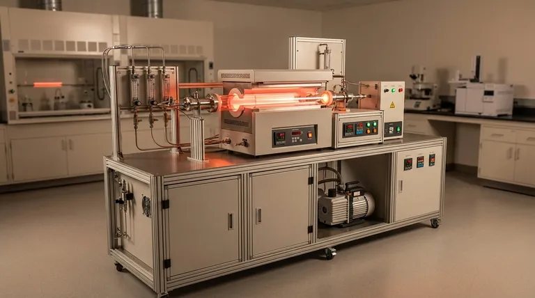
At its core, the process within a Chemical Vapor Deposition (CVD) machine uses gaseous chemicals to create a solid material layer on a surface. Volatile precursor gases are introduced into a reaction chamber where they encounter a heated object, known as the substrate. The heat triggers a chemical reaction or decomposition, causing a solid film to form and adhere to the substrate while gaseous byproducts are removed.
Chemical Vapor Deposition is not merely a coating technique; it is a material synthesis process. The fundamental principle is to control a chemical reaction at a molecular level, using a carefully managed environment of gas, heat, and pressure to build a high-purity solid film atom-by-atom on a target surface.
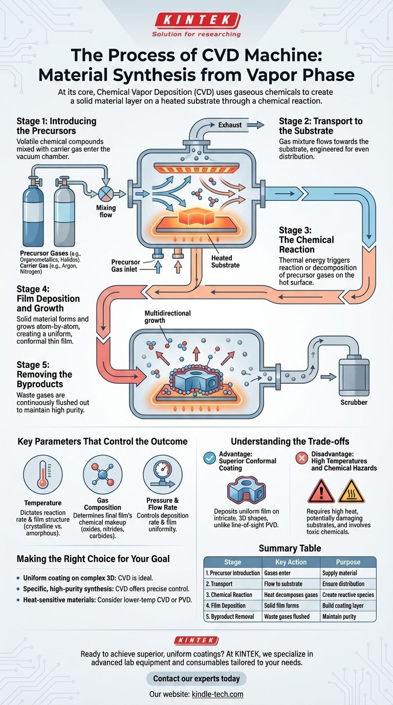
The Fundamental Stages of the CVD Process
Understanding CVD requires breaking it down into a sequence of distinct but interconnected stages. Each stage is critical for the successful formation of the desired material.
Stage 1: Introducing the Precursors
The process begins by introducing specific gases into a vacuum chamber. These are not just any gases; they are precursors, which are volatile chemical compounds containing the elements you wish to deposit.
These precursors are often mixed with a carrier gas (like argon or nitrogen), which helps transport them efficiently through the system.
Stage 2: Transport to the Substrate
This mixture of precursor and carrier gases flows through the chamber toward the substrate—the object that will be coated. The dynamics of this gas flow are engineered to ensure an even and consistent supply of reactive molecules to the substrate surface.
Stage 3: The Chemical Reaction
This is the heart of the CVD process. The substrate is heated to a precise temperature, providing the necessary thermal energy to drive a chemical reaction.
When the precursor gases come into contact with or pass near the hot substrate surface, they react or decompose. This breaks down the precursor molecules into their constituent parts.
Stage 4: Film Deposition and Growth
The desired solid product from the chemical reaction deposits directly onto the substrate's surface, forming a thin, solid film. This new layer grows as the process continues.
A key characteristic of CVD is that this deposition is multidirectional or conformal. The gas envelops the entire substrate, allowing the film to form uniformly over complex, non-flat geometries.
Stage 5: Removing the Byproducts
The chemical reaction also creates unwanted gaseous byproducts. These waste products are continuously flushed out of the reaction chamber by the steady gas flow, preventing them from contaminating the growing film and ensuring a high-purity final material.
Key Parameters That Control the Outcome
The quality and properties of the deposited film are not accidental. They are the direct result of carefully controlling several key variables within the CVD machine.
The Role of Temperature
Substrate temperature is arguably the most critical parameter. It dictates the rate of the chemical reaction and directly influences the final film's structure, such as whether it will be crystalline or amorphous.
The Importance of Gas Composition
The chemical makeup of the final film is determined by the precursor gases used. By selecting specific organometallic or halide compounds, engineers can create a vast range of inorganic materials, including oxides, nitrides, and carbides.
The Effect of Pressure and Flow Rate
The pressure inside the chamber and the flow rate of the gases affect how quickly the precursor molecules reach the substrate. These factors are tuned to control the deposition rate and the uniformity of the film across the entire substrate.
Understanding the Trade-offs
Like any technology, CVD has distinct advantages and limitations that make it suitable for some applications but not others. A common point of comparison is Physical Vapor Deposition (PVD).
Advantage: Superior Conformal Coating
CVD's greatest strength is its ability to deposit a uniform film on intricate, three-dimensional shapes. Because the precursor is a gas, it can reach every nook and cranny of a complex part.
This is a major advantage over line-of-sight techniques like PVD, which struggle to coat surfaces that are not directly facing the material source.
Disadvantage: High Temperatures and Chemical Hazards
The high temperatures required for many CVD processes can damage heat-sensitive substrates. While lower-temperature variants like Plasma-Enhanced CVD (PECVD) exist, heat is a common constraint.
Furthermore, many precursor chemicals are toxic, flammable, or corrosive, requiring stringent safety protocols and handling procedures.
Making the Right Choice for Your Goal
The decision to use CVD should be based on the specific properties required for your final product.
- If your primary focus is creating a uniform coating on a complex 3D object: CVD is the ideal choice due to its excellent conformal coverage.
- If your primary focus is synthesizing a specific, high-purity inorganic compound: CVD provides precise chemical control through precursor selection and reaction conditions.
- If your primary focus is working with heat-sensitive materials: You must consider lower-temperature CVD variants or evaluate alternative methods like PVD that operate at lower temperatures.
Ultimately, mastering the CVD process is about mastering the controlled synthesis of materials from the vapor phase.
Summary Table:
| Stage | Key Action | Purpose |
|---|---|---|
| 1. Precursor Introduction | Gases enter the chamber | Supply material for the film |
| 2. Transport | Gases flow to the substrate | Ensure even distribution |
| 3. Chemical Reaction | Heat decomposes gases on the substrate | Create reactive species for deposition |
| 4. Film Deposition | Solid material forms on the substrate | Build the desired coating layer by layer |
| 5. Byproduct Removal | Waste gases are flushed out | Maintain film purity and quality |
Ready to achieve superior, uniform coatings on complex components? The CVD process is key to creating high-purity materials for demanding applications. At KINTEK, we specialize in providing advanced lab equipment and consumables tailored to your laboratory's precise material synthesis needs.
Contact our experts today to discuss how our CVD solutions can enhance your research and development.
Visual Guide
Related Products
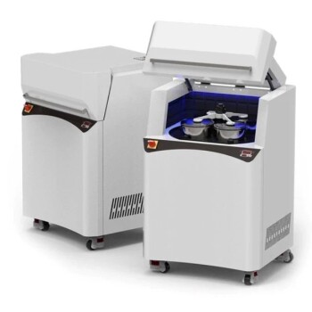
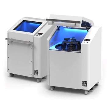
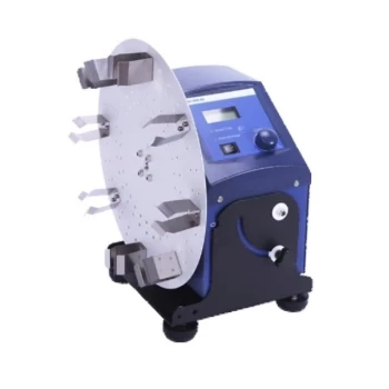
- HFCVD Machine System Equipment for Drawing Die Nano-Diamond Coating
- Microwave Plasma Chemical Vapor Deposition MPCVD Machine System Reactor for Lab and Diamond Growth
- Multi Heating Zones CVD Tube Furnace Machine Chemical Vapor Deposition Chamber System Equipment
- Chemical Vapor Deposition CVD Equipment System Chamber Slide PECVD Tube Furnace with Liquid Gasifier PECVD Machine
- CVD Diamond Dressing Tools for Precision Applications
People Also Ask
- How expensive is chemical vapor deposition? Understanding the True Cost of High-Performance Coating
- What is the full form of HFCVD? A Guide to Hot Filament Chemical Vapor Deposition
- What is the function of tungsten filaments in HFCVD? Powering Diamond Film Synthesis with Thermal Excitation
- What is the specific function of the metal filament in HF-CVD? Key Roles in Diamond Growth
- What is the chemical vapor deposition growth process? Build Superior Thin Films from the Atom Up