At its core, Chemical Vapor Deposition (CVD) for metals is a process of building a solid film from a chemical reaction in the gas phase. It involves introducing gaseous precursor chemicals into a reaction chamber, where they react and decompose on a heated substrate surface, leaving behind a thin, pure layer of the desired metal.
CVD is not a simple spray-coating process; it is a sophisticated method of atomic-scale construction. The process is governed by a precise sequence of mass transport and surface chemical reactions, where control over temperature, pressure, and gas flow is paramount to building a high-quality, uniform metal film.
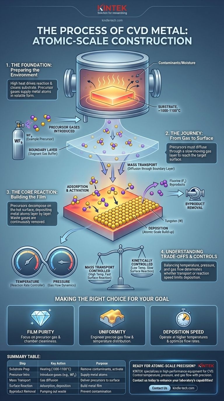
The Foundation: Preparing the Environment
Before any metal can be deposited, the stage must be perfectly set. This involves preparing both the object to be coated (the substrate) and introducing the necessary chemical ingredients.
The Critical Role of the Substrate
The substrate is the foundation upon which the new metal film is built. Its condition directly impacts the quality and adhesion of the final coating.
The substrate is placed inside a vacuum chamber and is typically heated to very high temperatures, often between 1000-1100°C. This extreme heat serves two purposes: it provides the necessary energy to drive the chemical reaction, and it helps burn off and remove contaminants like moisture or residual oxygen.
Introducing the Precursor Gases
With the substrate prepared, one or more reactive gases, known as precursors, are introduced into the chamber. These gases contain the atoms of the metal to be deposited, but in a volatile chemical form.
For example, to deposit a film of tungsten, a common precursor gas is tungsten hexafluoride (WF₆). The goal is to break this molecule apart at the substrate surface, leaving the tungsten behind.
The Journey: From Gas to Surface
Once the precursors are in the chamber, they must travel to the substrate surface for the reaction to occur. This transport phase is a critical step that dictates the uniformity and rate of deposition.
The Concept of the Boundary Layer
Directly above the substrate surface, a thin, slow-moving layer of gas called the boundary layer forms. This layer acts as a buffer between the free-flowing gases in the chamber and the static substrate.
For a reaction to happen, the precursor gas molecules must diffuse through this stagnant boundary layer to physically reach the surface.
Mass Transport to the Target
The movement of precursor gases from the main chamber flow, through the boundary layer, and to the substrate is known as mass transport. The efficiency of this step can often be the limiting factor for how fast the coating can grow.
The Core Reaction: Building the Film
This is the central event of the CVD process, where the gaseous chemicals are converted into a solid metal film on the substrate's surface.
Adsorption and Activation
When the precursor gas molecules reach the hot substrate, they stick to the surface in a process called adsorption. The thermal energy from the hot substrate activates the molecules, providing the energy needed to break their chemical bonds.
The Deposition Event
Once activated, the precursor molecules undergo a chemical reaction directly on the surface. They decompose, depositing the desired metal atoms onto the substrate. This process builds the film, layer by layer, with atomic-scale precision.
Removal of Byproducts
The chemical reaction also creates gaseous byproducts. For example, when tungsten hexafluoride (WF₆) deposits tungsten, it releases fluorine gas. These waste products are continuously pumped out of the reaction chamber to prevent them from contaminating the film or interfering with the deposition process.
Understanding the Trade-offs and Controls
CVD is a powerful technique, but its success hinges on balancing competing factors. The quality of the film is determined by which step in the process is the bottleneck.
Mass Transport vs. Kinetic Control
The speed of deposition is typically limited by one of two factors. At lower temperatures, the process is kinetically controlled, meaning the bottleneck is the speed of the chemical reaction on the surface itself.
At higher temperatures, the process becomes mass transport controlled. The surface reaction is very fast, so the bottleneck becomes the rate at which precursor gas can be supplied to the surface through the boundary layer. Understanding this balance is key to controlling film uniformity.
The Role of Temperature and Pressure
Temperature is the primary lever for controlling the reaction rate. Higher temperatures generally lead to faster deposition. Chamber pressure is also critical, as it influences gas flow dynamics and the concentration of reactants at the substrate surface.
Uniformity Is Not Guaranteed
Achieving a perfectly uniform coating thickness, especially over a complex shape, is a significant engineering challenge. It requires precise control over the temperature distribution across the substrate and the fluid dynamics of the gas flow within the chamber.
Making the Right Choice for Your Goal
The specific parameters of the CVD process are tuned based on the desired outcome for the metal film.
- If your primary focus is film purity: Your control over precursor gas purity and the cleanliness of the vacuum chamber is the most critical factor.
- If your primary focus is coating thickness uniformity: You must carefully engineer the gas flow dynamics and temperature distribution across the entire substrate.
- If your primary focus is deposition speed: You will need to operate at higher temperatures in a mass-transport-limited regime, which requires optimizing precursor concentration and flow rates.
Ultimately, Chemical Vapor Deposition is a process of disciplined, atomic-scale engineering, using chemistry and physics to construct materials from the ground up.
Summary Table:
| CVD Process Step | Key Action | Purpose |
|---|---|---|
| Substrate Preparation | Heating in vacuum chamber (1000-1100°C) | Remove contaminants, activate surface |
| Precursor Introduction | Introducing gases like WF₆ (for tungsten) | Supply metal atoms in volatile form |
| Mass Transport | Gas diffusion through boundary layer | Deliver precursors to substrate surface |
| Surface Reaction | Adsorption, decomposition, deposition | Build metal film layer by layer |
| Byproduct Removal | Pumping out waste gases (e.g., fluorine) | Prevent contamination, maintain process purity |
Ready to achieve atomic-scale precision in your metal deposition processes? KINTEK specializes in high-performance lab equipment and consumables for CVD applications. Our solutions are designed to help you control temperature, pressure, and gas flow with precision—ensuring high-purity, uniform metal films for your research or production needs.
Contact us today to discuss how our expertise can enhance your laboratory's capabilities!
Visual Guide
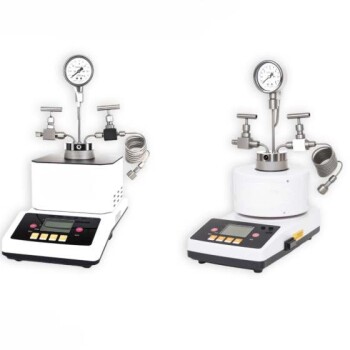
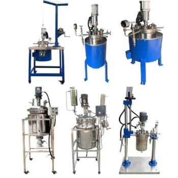
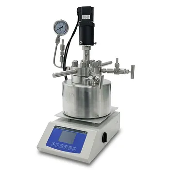
Related Products
- Cylindrical Resonator MPCVD Machine System Reactor for Microwave Plasma Chemical Vapor Deposition and Lab Diamond Growth
- Customer Made Versatile CVD Tube Furnace Chemical Vapor Deposition Chamber System Equipment
- Microwave Plasma Chemical Vapor Deposition MPCVD Machine System Reactor for Lab and Diamond Growth
- Split Chamber CVD Tube Furnace with Vacuum Station Chemical Vapor Deposition System Equipment Machine
- Multi Heating Zones CVD Tube Furnace Machine Chemical Vapor Deposition Chamber System Equipment
People Also Ask
- Why is argon-rich gas phase chemistry used for UNCD growth? Unlock Precision Nano-Diamond Synthesis
- What is MPCVD? Unlock Atom-by-Atom Precision for High-Purity Materials
- How is a diamond formed from CVD? The Science of Growing Diamonds Atom by Atom
- What are the primary advantages of the CVD method for growing diamonds? Engineering High-Purity Gems and Components
- How does chemical vapor deposition work for diamonds? Grow Lab-Created Diamonds Layer by Layer