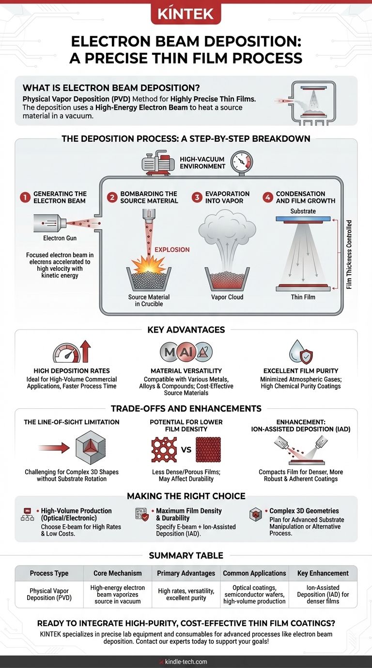
At its core, electron beam deposition is a physical vapor deposition (PVD) method used to create highly precise thin films. The process uses a high-energy beam of electrons to heat a source material inside a vacuum chamber until it evaporates. This resulting vapor then travels and condenses onto a target object, such as an optical lens or a semiconductor wafer, forming a thin, uniform coating.
Electron beam deposition is valued for its versatility, speed, and cost-effectiveness. It is a dominant technology for creating high-purity coatings in high-volume applications by using a focused energy beam to vaporize a wider and less expensive range of materials than many competing processes.
The Deposition Process: A Step-by-Step Breakdown
To understand its capabilities, it's essential to visualize the mechanics of the process, which takes place entirely within a high-vacuum environment to ensure film purity.
Step 1: Generating the Electron Beam
The process begins with an electron gun, which generates a focused stream of electrons. These electrons are accelerated to a very high velocity, imbuing them with significant kinetic energy.
Step 2: Bombarding the Source Material
This high-energy electron beam is magnetically guided to strike a source material—often in the form of powder or granules—held in a crucible. The intense and concentrated energy transfer is often described as bombardment.
Step 3: Evaporation into Vapor
The bombardment rapidly increases the temperature of the source material to its evaporation point. This transforms the solid material directly into a gaseous vapor, which then expands within the vacuum chamber.
Step 4: Condensation and Film Growth
The vapor travels in a straight line until it makes contact with the cooler substrate (the object being coated). Upon contact, the vapor condenses back into a solid state, forming a thin film. The thickness of this film is precisely controlled by monitoring the deposition rate and time.
Key Advantages of Electron Beam Deposition
Engineers and manufacturers choose E-beam deposition when certain outcomes are critical. Its primary advantages lie in its efficiency and flexibility.
High Deposition Rates
Compared to other methods like magnetron sputtering, E-beam deposition can achieve significantly higher deposition rates. This makes it ideal for high-volume commercial applications where process time per batch is a critical economic factor.
Material Versatility
The process is compatible with a vast array of materials, including metals, alloys, and dielectric compounds. Crucially, the source materials are often less expensive than the specialized "targets" required for sputtering, lowering overall production costs.
Excellent Film Purity
Because the process occurs in a high vacuum, the risk of atmospheric gases becoming trapped in the film is minimized. This results in coatings with very high chemical purity.
Understanding the Trade-offs and Enhancements
No single technology is perfect for every scenario. Understanding the limitations of E-beam deposition is key to using it effectively.
The Line-of-Sight Limitation
E-beam is a line-of-sight process. The evaporated material travels in a straight path from the source to the substrate. This can make it challenging to uniformly coat complex, three-dimensional shapes without sophisticated substrate rotation and tilting mechanisms.
Potential for Lower Film Density
Under standard conditions, the resulting film can sometimes be less dense and more porous than films created by higher-energy processes like sputtering. This can affect the coating's mechanical durability and environmental stability.
Enhancement: Ion-Assisted Deposition (IAD)
To overcome the density limitation, E-beam systems are often enhanced with an ion source. This secondary beam of ions bombards the growing film during deposition. This action compacts the film, resulting in a denser, more robust, and more adherent coating with reduced internal stress.
Making the Right Choice for Your Application
Selecting a deposition method requires aligning the technology's strengths with your project's primary goal.
- If your primary focus is high-volume production of optical or electronic coatings: E-beam is a powerful candidate due to its high deposition rates and the low cost of its source materials.
- If your primary focus is maximum film density and durability from the start: You should specify an E-beam process enhanced with Ion-Assisted Deposition (IAD) to achieve a more robust and stable coating.
- If your primary focus is coating complex 3D geometries: You must plan for E-beam's line-of-sight nature with advanced substrate manipulation or consider an alternative, more conformal process.
By understanding its mechanics and inherent trade-offs, you can effectively leverage electron beam deposition to achieve precise, high-quality thin films for your specific needs.
Summary Table:
| Key Aspect | Description |
|---|---|
| Process Type | Physical Vapor Deposition (PVD) |
| Core Mechanism | High-energy electron beam vaporizes a source material in a vacuum. |
| Primary Advantages | High deposition rates, material versatility, excellent film purity. |
| Common Applications | Optical coatings, semiconductor wafers, high-volume commercial production. |
| Key Enhancement | Ion-Assisted Deposition (IAD) for denser, more robust films. |
Ready to integrate high-purity, cost-effective thin film coatings into your laboratory workflow? KINTEK specializes in providing the precise lab equipment and consumables you need for advanced processes like electron beam deposition. Whether you're in R&D or high-volume production, our solutions are designed to enhance your efficiency and results. Contact our experts today to discuss how we can support your specific application goals!
Visual Guide
Related Products
- Electron Beam Evaporation Coating Oxygen-Free Copper Crucible and Evaporation Boat
- RF PECVD System Radio Frequency Plasma-Enhanced Chemical Vapor Deposition RF PECVD
- Electron Beam Evaporation Coating Tungsten Crucible and Molybdenum Crucible for High Temperature Applications
- Electron Beam Evaporation Coating Conductive Boron Nitride Crucible BN Crucible
- Electron Beam Evaporation Coating Gold Plating Tungsten Molybdenum Crucible for Evaporation
People Also Ask
- What is the deposition rate of e-beam evaporation? Control Thin Film Quality and Speed
- How is an electron beam evaporator cooled during deposition? Essential Thermal Management for Stable Processes
- What is the current of e-beam evaporation? A Guide to High-Purity Thin Film Deposition
- What is the temperature of e-beam evaporation? Mastering the Two-Zone Thermal Process for Precision Films
- What are the applications of e-beam evaporation? Achieve High-Purity Coatings for Optics & Electronics


