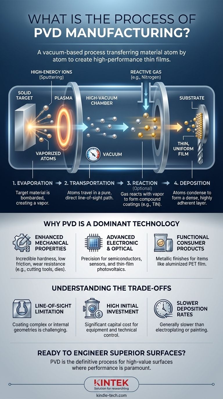
At its core, Physical Vapor Deposition (PVD) is a vacuum-based manufacturing process that transfers a material atom by atom from a solid source to a substrate, creating an exceptionally thin and high-performance coating. The process can be broken down into four fundamental stages: evaporation, transportation, reaction, and deposition. During evaporation, a target material is bombarded with a high-energy source to release atoms, which then travel through a vacuum, often reacting with specific gases, before condensing onto the target object as a durable film.
PVD is not a single method but a family of processes used to engineer surfaces at the atomic level. Its defining characteristic is the creation of a high-purity, high-performance thin film by depositing vaporized material onto a substrate within a controlled vacuum environment.
Deconstructing the PVD Process
The PVD process is a sequence of highly controlled physical events that occur inside a vacuum chamber. Understanding these steps clarifies how PVD achieves its unique coating properties.
Step 1: Evaporation (Creating the Vapor)
The process begins by turning a solid source material, known as the target, into a vapor. This is not achieved through simple melting but by bombarding the target with high energy.
The most common method is sputtering, where a high-energy plasma (typically from an inert gas like argon) is created. Ions from this plasma strike the target with enough force to dislodge or "sputter" individual atoms from its surface.
Step 2: Transportation (Moving Through a Vacuum)
The newly liberated atoms or molecules travel from the target toward the substrate (the object being coated). This journey takes place within a high-vacuum chamber.
The vacuum is critical. It removes air and other gas particles that would otherwise collide with and contaminate the vaporized coating material, ensuring a pure and direct "line-of-sight" path to the substrate.
Step 3: Reaction (Optional but Powerful)
To create highly durable compound coatings, a reactive gas is often introduced into the chamber during the transportation stage.
For example, by introducing nitrogen, metal atoms from the target can react to form a metal nitride film. Similarly, introducing oxygen creates a metal oxide. This step allows for the creation of specific ceramic coatings like Titanium Nitride (TiN) or Titanium Carbo-Nitride (TiCN) from a solid titanium target.
Step 4: Deposition (Building the Film)
When the vaporized atoms reach the cooler substrate, they condense and form a thin, highly adherent film. This film builds up atom by atom, creating a very dense and uniform layer.
This atomic deposition process results in a coating with a powerful bond to the substrate surface, which is responsible for the exceptional durability associated with PVD finishes.
Why PVD Is a Dominant Coating Technology
PVD is chosen when standard coating methods cannot meet the demanding requirements for mechanical, optical, or electronic performance.
For Enhanced Mechanical Properties
PVD coatings are incredibly hard and have a low coefficient of friction. This is why they are used to coat metalworking cutting tools and high-wear industrial components. A thin layer of Titanium Nitride (TiN) can dramatically extend the life of a drill bit.
For Advanced Electronic and Optical Functions
The precision of PVD makes it essential for manufacturing semiconductor devices and microchips. It is used to deposit ultra-thin layers of conductive metals like copper, platinum, or tungsten.
This same precision is used for creating thin-film photovoltaic cells (solar panels), where materials like copper, indium, and gallium are deposited onto glass or plastic substrates.
For Functional Consumer and Industrial Products
PVD is also behind the metallic finish on many common items. For example, aluminized PET film, used for food packaging and balloons, is created using PVD to deposit a thin layer of aluminum.
Understanding the Trade-offs
While powerful, PVD is not the right solution for every application. Objectively evaluating its limitations is crucial.
Line-of-Sight Limitation
Because the vaporized material travels in a straight line, PVD is fundamentally a line-of-sight process. Coating complex, non-visible, or internal geometries is challenging and may require sophisticated fixtures to rotate the part during deposition.
High Initial Investment
PVD equipment, including vacuum chambers, power supplies, and plasma sources, represents a significant capital investment. The process complexity requires a high degree of technical control, adding to the operational cost.
Slower Deposition Rates
Compared to conventional coating methods like electroplating or painting, PVD is generally a slower process. This makes it less economical for applications that require very thick coatings or extremely high throughput.
Making the Right Choice for Your Application
Selecting a coating technology depends entirely on your end goal and operational constraints.
- If your primary focus is extreme hardness and wear resistance: PVD is the superior choice for applications like tools, dies, and high-performance mechanical components where durability is paramount.
- If your primary focus is creating a precise, pure, and ultra-thin film: PVD is the industry standard for semiconductors, optical lenses, sensors, and solar cells where atomic-level control is non-negotiable.
- If your primary focus is a general-purpose, low-cost coating on a simple shape: Consider traditional methods like electroplating or wet painting, which may be more cost-effective if extreme performance is not required.
Ultimately, PVD is the definitive process for engineering high-value surfaces where performance cannot be compromised.
Summary Table:
| PVD Process Stage | Key Action | Purpose/Outcome |
|---|---|---|
| 1. Evaporation | Target material is bombarded with high energy (e.g., sputtering). | Creates a vapor of source material atoms. |
| 2. Transportation | Vaporized atoms travel through a high-vacuum chamber. | Ensures a pure, direct path to the substrate, free from contamination. |
| 3. Reaction (Optional) | Reactive gas (e.g., nitrogen, oxygen) is introduced. | Forms compound coatings like Titanium Nitride (TiN) for enhanced properties. |
| 4. Deposition | Atoms condense onto the cooler substrate. | Builds a dense, uniform, and highly adherent thin film atom by atom. |
Ready to Engineer Superior Surfaces with PVD?
PVD technology is essential for creating high-performance coatings that offer exceptional hardness, wear resistance, and precision. Whether you are developing advanced cutting tools, semiconductor devices, or durable consumer products, the right PVD process is key to your success.
KINTEK specializes in providing advanced lab equipment and consumables for your PVD and surface engineering needs. Our expertise helps laboratories and manufacturers achieve precise, reliable, and high-quality results.
Contact us today to discuss how we can support your specific application and help you leverage the full potential of PVD technology.
Visual Guide
Related Products
- RF PECVD System Radio Frequency Plasma-Enhanced Chemical Vapor Deposition RF PECVD
- VHP Sterilization Equipment Hydrogen Peroxide H2O2 Space Sterilizer
- Chemical Vapor Deposition CVD Equipment System Chamber Slide PECVD Tube Furnace with Liquid Gasifier PECVD Machine
- Split Chamber CVD Tube Furnace with Vacuum Station Chemical Vapor Deposition System Equipment Machine
- 1400℃ Controlled Atmosphere Furnace with Nitrogen and Inert Atmosphere
People Also Ask
- How does RF power create plasma? Achieve Stable, High-Density Plasma for Your Applications
- What is an example of PECVD? RF-PECVD for High-Quality Thin Film Deposition
- What are the benefits of PECVD? Achieve Superior Low-Temperature Thin Film Deposition
- What are the advantages of PECVD? Enable Low-Temperature, High-Quality Thin-Film Deposition
- What are the applications of PECVD? Essential for Semiconductors, MEMS, and Solar Cells