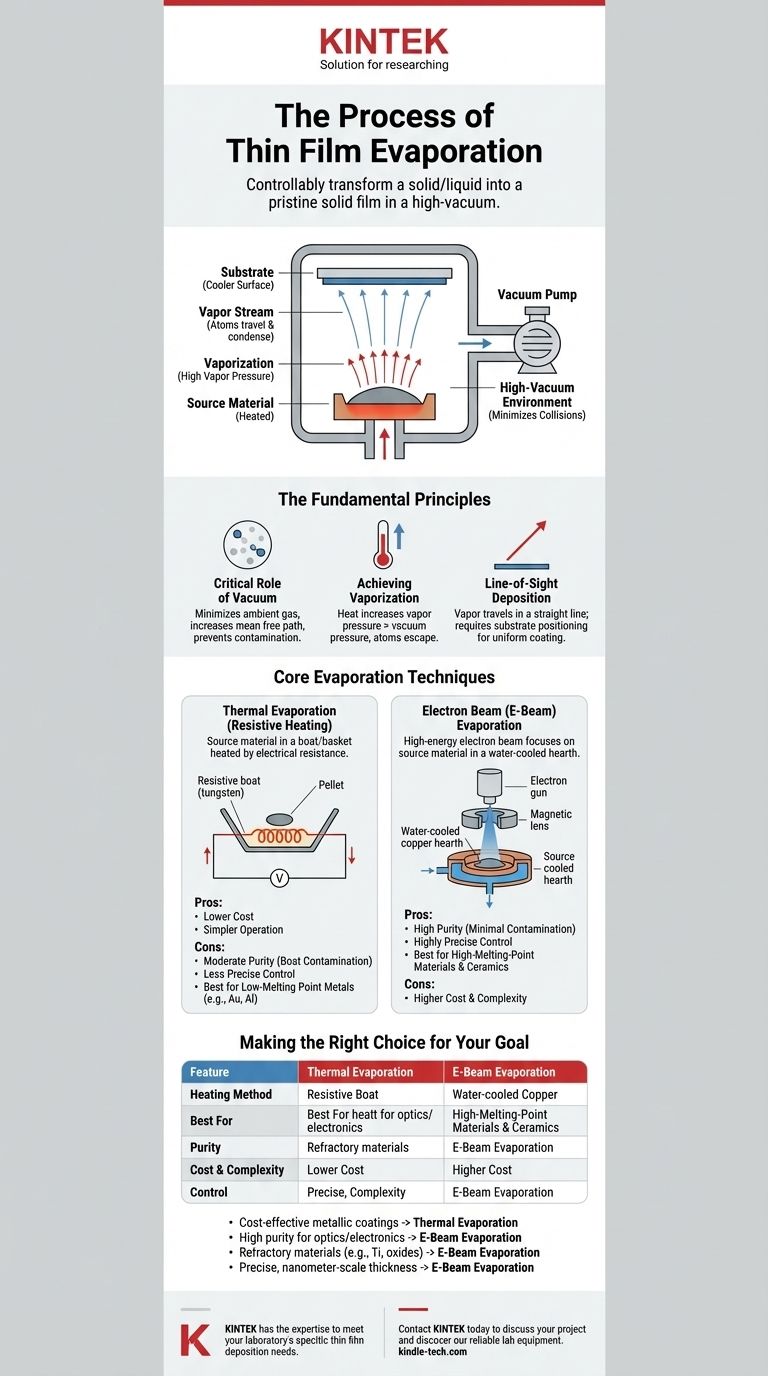
In short, thin film evaporation is a process where a source material is heated in a high-vacuum chamber until its atoms turn into a vapor. This vapor then travels and condenses onto a cooler surface, called a substrate, forming an ultra-thin, high-purity film. The entire process is a type of Physical Vapor Deposition (PVD).
The core principle of thin film evaporation is straightforward: controllably transform a solid or liquid material into a gas within a vacuum and then re-condense it as a pristine solid film on a target. The key differences in technique simply come down to how the material is heated.
The Fundamental Principles of Evaporation
To truly understand the process, you must first grasp the environment and physics that make it possible. The method is more than just boiling a material; it is a highly controlled phase transition.
The Critical Role of the Vacuum
The process occurs in a high-vacuum environment. This is not an optional detail—it is fundamental to success.
A vacuum minimizes the number of ambient gas molecules in the chamber. This ensures that evaporated atoms travel directly to the substrate with few or no collisions, a concept known as increasing the mean free path. This prevents contamination and unwanted chemical reactions, resulting in a much purer final film.
Achieving Vaporization
All materials have a vapor pressure, which is the pressure exerted by their gaseous phase. By applying energy in the form of heat, we increase this vapor pressure.
When the material's vapor pressure surpasses the pressure of the surrounding vacuum chamber, atoms gain enough energy to escape the source and travel through the chamber.
Line-of-Sight Deposition
Once vaporized, atoms travel in a straight line from the source to the substrate. This line-of-sight characteristic means the process is highly directional.
The substrate is strategically positioned above the source to intercept this vapor stream. This is why uniform coating on complex, three-dimensional shapes can be challenging without substrate rotation or movement.
Core Evaporation Techniques
While the principle remains the same, the method used to deliver heat to the source material defines the two primary techniques.
Thermal Evaporation (Resistive Heating)
This is the conceptually simpler method. The source material, often in pellet or powder form, is placed in a small container called a "boat" or "basket."
This boat is typically made of a refractory metal like tungsten or molybdenum. A high electrical current is passed through the boat, causing it to heat up due to its own electrical resistance. This heat is then transferred to the source material, causing it to melt and evaporate.
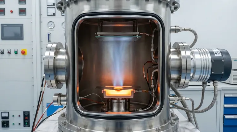
Electron Beam (E-Beam) Evaporation
In this more advanced technique, the source material is held in a water-cooled copper hearth or crucible. A high-energy electron beam is generated and magnetically guided to strike the surface of the source material.
The intense, focused energy of the electron beam heats a very small spot on the material to an extremely high temperature, causing localized evaporation. Because the crucible is water-cooled, only the source material gets hot, not the container.
Understanding the Trade-offs
Choosing between thermal and e-beam evaporation depends entirely on your material requirements, purity needs, and budget.
Purity and Contamination
E-beam evaporation generally produces higher-purity films. Since the electron beam only heats the source material, contamination from the container (crucible) is negligible.
Thermal evaporation carries a higher risk of contamination. The heated boat can sometimes react with or outgas, introducing impurities from the boat material itself into the vapor stream and the final film.
Material Compatibility
Thermal evaporation is well-suited for materials with relatively low melting points, like gold, aluminum, or silver. Heating materials with very high melting points can destroy the boat.
E-beam evaporation is the superior choice for high-melting-point (refractory) materials and ceramics. The focused energy of the electron beam can vaporize nearly any material without damaging the system.
Process Control and Cost
Thermal evaporation systems are simpler, less expensive to build, and easier to operate. However, controlling the evaporation rate with precision can be difficult.
E-beam evaporation provides far more precise control over the deposition rate and film thickness. This precision comes with higher equipment cost and system complexity.
Making the Right Choice for Your Goal
Your application's specific needs will dictate the ideal evaporation technique.
- If your primary focus is cost-effectiveness for simple metallic coatings: Thermal evaporation offers a straightforward and economical solution.
- If your primary focus is high purity for advanced optics or electronics: E-beam evaporation is the necessary choice to avoid contamination.
- If your primary focus is depositing refractory materials like titanium or oxides: E-beam evaporation is the only viable method due to its high-energy heating capability.
- If your primary focus is precise, repeatable control over nanometer-scale film thickness: The advanced monitoring and control of an e-beam system are essential.
Ultimately, understanding these methods allows you to select the right tool to reliably transform a raw material into a high-performance thin film.
Summary Table:
| Feature | Thermal Evaporation | E-Beam Evaporation |
|---|---|---|
| Heating Method | Resistive heating of a metal boat | Focused electron beam on the source material |
| Best For | Low-melting-point metals (e.g., Au, Al) | High-purity films & refractory materials (e.g., Ti, oxides) |
| Purity | Moderate (risk of boat contamination) | High (minimal contamination) |
| Cost & Complexity | Lower cost, simpler operation | Higher cost, more complex system |
| Control | Less precise evaporation rate control | Highly precise rate and thickness control |
Ready to Achieve Superior Thin Films for Your Application?
Whether you need cost-effective thermal evaporation for simple coatings or high-purity e-beam evaporation for advanced R&D and production, KINTEK has the expertise and equipment to meet your laboratory's specific thin film deposition needs.
Contact KINTEK today to discuss your project and discover how our reliable lab equipment can help you deposit consistent, high-performance thin films.
Visual Guide
Related Products
- Aluminized Ceramic Evaporation Boat for Thin Film Deposition
- Tungsten Evaporation Boat for Thin Film Deposition
- Electron Beam Evaporation Coating Oxygen-Free Copper Crucible and Evaporation Boat
- Molybdenum Tungsten Tantalum Evaporation Boat for High Temperature Applications
- Hemispherical Bottom Tungsten Molybdenum Evaporation Boat
People Also Ask
- Why is an alumina boat and Ti3AlC2 powder bed necessary for Ti2AlC sintering? Protect MAX Phase Purity
- What is the source of evaporation for thin film? Choosing Between Thermal and E-Beam Methods
- What are thin films deposited by evaporation? A Guide to High-Purity Coating
- Why is an alumina boat selected for catalyst precursors? Ensure Sample Purity at 1000 °C
- What is the widely used boat made of in thermal evaporation? Choosing the Right Material for High-Purity Deposition