The fundamental purpose of Chemical Vapor Deposition (CVD) is to create exceptionally pure, high-performance thin films and coatings on a material's surface. It is a manufacturing process that uses reactive gases in a vacuum to build a solid material, layer by layer, directly onto a component. This method allows for the creation of surfaces with enhanced properties like extreme durability, corrosion resistance, or specific electronic characteristics.
CVD is more than a simple coating technique; it is a precision manufacturing process for building materials from a gaseous state. This allows engineers to create ultra-pure, durable, and highly uniform surfaces with specific properties that the original bulk material lacks.
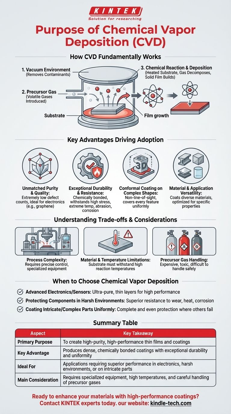
How CVD Fundamentally Works
Chemical Vapor Deposition is a process defined by a controlled chemical reaction that results in a solid deposit. The entire process takes place within a vacuum chamber to ensure purity.
The Vacuum Environment
First, a component (or "substrate") is placed into a vacuum chamber. This controlled environment is critical for removing contaminants and ensuring that the only chemical reactions that occur are the ones intended.
The Precursor Gas
Next, one or more volatile gases, known as precursors, are introduced into the chamber. These gases contain the specific atoms (like carbon, silicon, or titanium) that will form the final coating.
The Chemical Reaction and Deposition
The chamber and substrate are heated to a precise reaction temperature. This energy causes the precursor gases to react or decompose, breaking their chemical bonds. The freed atoms then bond with the substrate's surface, creating a thin, solid film that gradually builds in thickness over time.
Key Advantages Driving its Adoption
CVD is chosen over other methods when the quality and performance of the surface are paramount. Its advantages stem directly from its unique gas-phase deposition mechanism.
Unmatched Purity and Quality
Because the process starts with highly pure gases in a vacuum, CVD can produce films with extremely low defect counts. This is why it is a leading method for manufacturing high-performance materials like graphene for electronics and sensors.
Exceptional Durability and Resistance
The films created by CVD are not merely painted on; they are chemically bonded to the substrate. This results in dense, durable coatings that can withstand high-stress environments, extreme temperatures, abrasion, and corrosion.
Conformal Coating on Complex Shapes
Unlike line-of-sight processes like spraying, the precursor gases in CVD flow around and into every feature of a component. This "non-line-of-sight" nature allows it to deposit a perfectly uniform coating on even the most complex and intricate surfaces.
Material and Application Versatility
The process is incredibly versatile. It can be used to coat a wide range of materials, including metals, ceramics, and glass. By changing the precursor gases, the resulting film can be optimized for vastly different applications, from ultra-thin conductive layers in circuits to thick, wear-resistant industrial coatings.
Understanding the Trade-offs and Considerations
While powerful, CVD is a sophisticated process with specific requirements that make it unsuitable for every application. Understanding these factors is key to knowing when to leverage it.
Process Complexity
CVD requires precise control over temperature, pressure, and gas flow rates within a high-vacuum system. This level of control necessitates specialized, and often expensive, equipment compared to simpler coating methods.
Material and Temperature Limitations
The substrate material must be able to withstand the high reaction temperatures required for the precursor gases to decompose. This can limit the types of materials that can be effectively coated without being damaged.
Precursor Gas Handling
The volatile gases used as precursors can be expensive, toxic, or difficult to handle safely. This adds logistical and safety considerations to the manufacturing process.
When to Choose Chemical Vapor Deposition
The decision to use CVD should be based on the final performance requirements of the component.
- If your primary focus is advanced electronics or sensors: CVD is the ideal choice for creating the ultra-pure, defect-free, and exceptionally thin material layers required for high performance.
- If your primary focus is protecting components in harsh environments: The dense, durable, and chemically bonded coatings from CVD provide superior resistance to wear, heat, and corrosion.
- If your primary focus is coating intricate or complex parts uniformly: CVD's ability to conformally coat any exposed surface ensures complete and even protection where other methods would fail.
Ultimately, CVD empowers engineers to fundamentally enhance a material's surface, unlocking performance that the bulk material alone cannot provide.
Summary Table:
| Aspect | Key Takeaway |
|---|---|
| Primary Purpose | To create high-purity, high-performance thin films and coatings on a substrate's surface. |
| Key Advantage | Produces dense, chemically bonded coatings with exceptional durability and uniformity, even on complex shapes. |
| Ideal For | Applications requiring superior performance in electronics, harsh environments, or on intricate parts. |
| Main Consideration | Requires specialized equipment, high temperatures, and careful handling of precursor gases. |
Ready to enhance your materials with high-performance coatings?
KINTEK specializes in providing the advanced lab equipment and consumables needed for precise Chemical Vapor Deposition processes. Whether you are developing next-generation electronics or require durable coatings for industrial components, our expertise can help you achieve superior results.
Contact our experts today to discuss how our solutions can meet your specific laboratory and manufacturing needs.
Visual Guide
Related Products
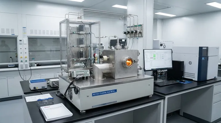
- Chemical Vapor Deposition CVD Equipment System Chamber Slide PECVD Tube Furnace with Liquid Gasifier PECVD Machine
- Microwave Plasma Chemical Vapor Deposition MPCVD Machine System Reactor for Lab and Diamond Growth
- 915MHz MPCVD Diamond Machine Microwave Plasma Chemical Vapor Deposition System Reactor
- Customer Made Versatile CVD Tube Furnace Chemical Vapor Deposition Chamber System Equipment
- HFCVD Machine System Equipment for Drawing Die Nano-Diamond Coating
People Also Ask
- Why is Chemical Vapor Deposition (CVD) equipment uniquely suited for constructing hierarchical superhydrophobic structures?
- What is the chemical vapor deposition growth process? Build Superior Thin Films from the Atom Up
- What are the core advantages of PE-CVD in OLED encapsulation? Protect Sensitive Layers with Low-Temp Film Deposition
- What is plasma enhanced chemical vapor deposition PECVD equipment? A Guide to Low-Temperature Thin Film Deposition
- What are the advantages of chemical vapor deposition? Achieve Superior Thin Films for Your Lab


