When we speak of the "range" of thin films, we are not referring to a single metric but to the vast scope of this technology across four key dimensions. Its physical thickness typically spans from a few nanometers to several micrometers. More importantly, its range encompasses an enormous variety of materials, a wide spectrum of functional properties, and a constantly expanding list of high-tech applications, from microchips to medical devices.
The core concept of thin film technology is not its physical dimension alone, but its function as a versatile platform. By precisely controlling material layers at the nanoscale, we can engineer unique optical, electrical, and mechanical properties that are impossible to achieve in bulk materials.
The Defining "Range": Film Thickness
The most literal interpretation of "range" is thickness. This dimension is the foundation from which all other properties emerge.
From Single Atoms to Micrometers
A thin film is a layer of material whose thickness can range from a single layer of atoms (fractions of a nanometer) up to several micrometers (µm).
Most industrial applications operate in the range of 10 nanometers to 10 micrometers. This scale is the sweet spot where a material is thin enough to exhibit unique properties but thick enough to be robust and functional.
Why Thickness Matters
At these small dimensions, effects that are negligible in bulk materials become dominant. This includes quantum mechanical phenomena, optical interference, and unique stress-strain relationships, allowing engineers to fine-tune a material's performance by simply adjusting its thickness.
The Range of Materials and Processes
The versatility of thin film technology is directly tied to the wide array of materials that can be deposited and the precision of the methods used to do so.
From Metals to Advanced Ceramics
Virtually any class of material can be made into a thin film. The references highlight a broad selection including:
- Metals: Aluminum, refractory metals
- Dielectrics & Ceramics: Silicon oxides, nitrides (TiN)
- Semiconductors: Silicon, Germanium, compound semiconductors (GaAs)
- Specialty Materials: Diamond-like carbon (DLC), and emerging amorphous oxides
This material diversity allows for the creation of coatings tailored to nearly any engineering challenge.
The Processes That Enable Precision
Creating these films requires highly controlled environments and sophisticated equipment. Key methods include:
- Chemical Vapor Deposition (CVD): Uses precursor gases to "grow" a film on a surface, ideal for creating uniform, high-purity layers.
- Physical Vapor Deposition (PVD): Involves vaporizing a solid material (sputtering or evaporation) in a vacuum and letting it condense on a substrate, excellent for metals and hard coatings.
- Ion Implantation: Injects charged atoms (ions) into a surface to change its chemical and physical properties.
The Spectrum of Achievable Properties
Depositing a material as a thin film is done to achieve specific functional properties that differ from the bulk material.
Manipulating Optical Properties
Thin films are critical for controlling light. They can be engineered to be highly transparent for displays, anti-reflective for lenses, or highly reflective for mirrors.
Controlling Electrical Behavior
A film's electrical properties can be precisely tuned. They can act as conductors in microchip wiring, insulators (dielectrics) in capacitors, or semiconductors in transistors.
Enhancing Mechanical Durability
Thin films are often used as protective coatings. Materials like titanium nitride (TiN) and diamond-like carbon (DLC) create ultra-hard, scratch-resistant, and low-friction surfaces for cutting tools and wear components.
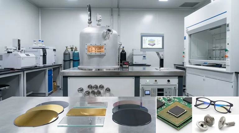
The Breadth of Modern Applications
The combination of materials and properties gives thin films an exceptionally broad range of applications that define modern technology.
- Semiconductor Manufacturing: Forms the basis of every integrated circuit, creating the transistors, wires, and insulators on a silicon wafer.
- Displays & Optics: Enables everything from flat-panel TVs and smartphone screens to coated eyeglasses and high-performance lenses.
- Data Storage: Used to create the magnetic layers in hard drives and the phase-change layers in optical discs.
- Medical Devices: Provides biocompatible coatings for implants and durable, sterile surfaces for surgical tools.
Understanding the Inherent Trade-offs
While powerful, thin film technology is not without its challenges and limitations. Understanding these is key to its successful application.
Cost and Complexity
The equipment for deposition processes like CVD and PVD is expensive and requires significant expertise to operate and maintain. This creates a high barrier to entry for manufacturing.
Substrate Dependency
Thin films must be deposited onto a substrate (like a silicon wafer or piece of glass). The film's adhesion, stress, and final properties are highly dependent on the choice of this substrate and its surface preparation.
Durability and Stability
Extremely thin layers can be fragile and susceptible to scratches, delamination, or environmental degradation. Achieving a desired property (like transparency) often involves a trade-off with long-term durability.
How to Frame 'Range' for Your Goal
The "range" of thin film technology is best understood through the lens of your specific objective.
- If your primary focus is materials science or R&D: The range of new material combinations, like the amorphous oxides for transparent transistors, is the most critical area for innovation.
- If your primary focus is manufacturing and engineering: The range of deposition processes (CVD, PVD) and your ability to control them to achieve consistent film properties is your key variable.
- If your primary focus is product development: The range of applications, from optics to electronics and beyond, defines the market opportunities where this technology can provide a competitive advantage.
Ultimately, thin film is a foundational technology that gives us the power to engineer matter at the microscopic scale.
Summary Table:
| Aspect of Range | Key Details |
|---|---|
| Thickness | Single atoms (<1 nm) to several micrometers (µm) |
| Materials | Metals (Al, Ti), Ceramics (TiN), Semiconductors (Si, GaAs), DLC |
| Key Properties | Optical (transparency), Electrical (conductivity), Mechanical (hardness) |
| Primary Applications | Semiconductors, Displays, Data Storage, Medical Devices |
Ready to engineer superior surfaces with precision thin films? KINTEK specializes in advanced lab equipment and consumables for thin film deposition (CVD, PVD) and analysis. Whether you're in R&D or manufacturing, our solutions help you achieve consistent, high-performance coatings. Contact our experts today to discuss how we can support your specific laboratory needs and accelerate your innovation.
Visual Guide

Related Products
- Aluminized Ceramic Evaporation Boat for Thin Film Deposition
- Tungsten Evaporation Boat for Thin Film Deposition
- Electron Beam Evaporation Coating Oxygen-Free Copper Crucible and Evaporation Boat
- Molybdenum Tungsten Tantalum Evaporation Boat for High Temperature Applications
- Aluminum-Plastic Flexible Packaging Film for Lithium Battery Packaging
People Also Ask
- What is the widely used boat made of in thermal evaporation? Choosing the Right Material for High-Purity Deposition
- Why are high-purity ceramic boats used for lignin activation? Ensure Purity & Thermal Stability
- What are thin films deposited by evaporation? A Guide to High-Purity Coating
- What are the alternatives to sputtering? Choose the Right Thin Film Deposition Method
- What are the applications of thin films deposition? Unlock New Possibilities for Your Materials


