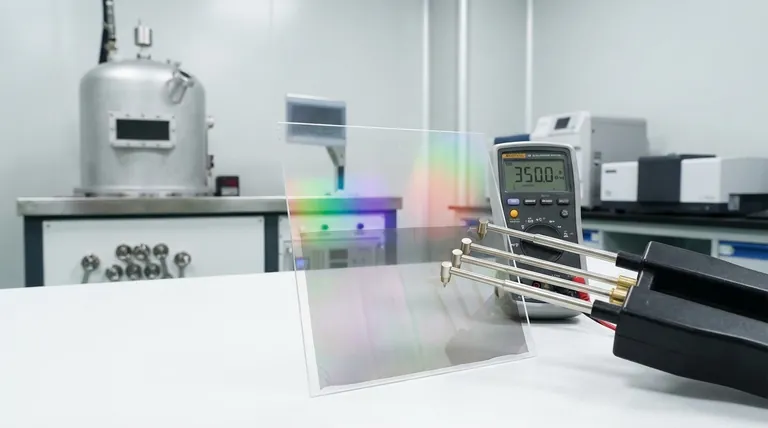
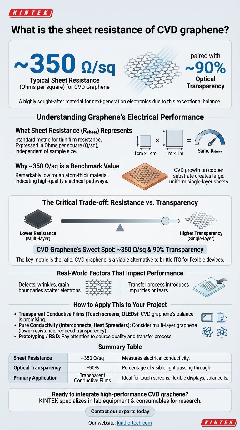
For Chemical Vapor Deposition (CVD) graphene, a typical sheet resistance value is approximately 350 Ω/sq (Ohms per square). This figure is particularly significant because it is achieved while the material maintains about 90% optical transparency. This combination of electrical conductivity and transparency is the primary reason CVD graphene is a highly sought-after material for next-generation electronics.
The specific value of sheet resistance is only half the story. The true measure of CVD graphene's performance lies in its exceptional balance between low electrical resistance and high optical transparency, making it a prime candidate for transparent conductive films.
Understanding Graphene's Electrical Performance
What Sheet Resistance (Rsheet) Represents
Sheet resistance is the standard metric used to measure the electrical resistance of thin films, like graphene. It is expressed in Ohms per square (Ω/sq).
This unit simplifies comparisons because it is independent of the sample's size. A 1cm x 1cm square of a material will have the same sheet resistance as a 1m x 1m square of the same material and thickness.
Why ~350 Ω/sq is a Benchmark Value
For a material that is only a single atom thick, a sheet resistance of 350 Ω/sq is remarkably low. It demonstrates high-quality electrical pathways across the graphene sheet.
This performance is largely credited to the CVD growth process on a copper substrate. The copper acts as a catalyst, enabling the formation of large, relatively uniform, single-layer graphene sheets essential for consistent conductivity.
The Critical Trade-off: Resistance vs. Transparency
The Core Performance Metric for Transparent Conductors
In applications like touch screens, solar cells, or flexible displays, conductivity alone is not enough. The material must also be transparent.
Therefore, the most important metric is the ratio of transparency to sheet resistance. A material is considered high-performance if it can carry a current with minimal resistance while letting most light pass through.
The Significance of 90% Transparency
The 350 Ω/sq value for CVD graphene is impressive because it is paired with 90% transparency. This level of performance makes it a viable alternative to traditional materials like Indium Tin Oxide (ITO), which is more brittle and less suitable for flexible devices.
Theoretically, a perfect single layer of graphene absorbs only 2.3% of visible light, so a 90% transparency figure indicates a high-quality, predominantly single-layer film.
Real-World Factors That Impact Performance
The ideal value of 350 Ω/sq can be affected by several factors. Defects, wrinkles, or grain boundaries in the graphene lattice can scatter electrons and increase resistance.
Furthermore, the process of transferring the graphene from its copper growth substrate to a target substrate (like glass or plastic) can introduce impurities or tears, which also degrade electrical performance.
How to Apply This to Your Project
- If your primary focus is transparent conductive films (e.g., touch screens, OLEDs): CVD graphene's balance of ~350 Ω/sq resistance and 90% transparency makes it one of the most promising materials available.
- If your primary focus is purely conductivity (e.g., interconnects, heat spreaders): You may explore multi-layer graphene, which offers lower sheet resistance but at the cost of reduced transparency.
- If you are prototyping or in R&D: Pay close attention to the quality of your graphene source and the transfer process, as these will be the dominant factors determining the final sheet resistance of your device.
Ultimately, understanding this balance between conductivity and transparency is key to leveraging CVD graphene's unique potential in your application.
Summary Table:
| Key Metric | Typical Value for CVD Graphene | Importance |
|---|---|---|
| Sheet Resistance | ~350 Ω/sq | Measures electrical conductivity of the thin film. |
| Optical Transparency | ~90% | Percentage of visible light that passes through. |
| Primary Application | Transparent Conductive Films | Ideal for touch screens, flexible displays, and solar cells. |
Ready to integrate high-performance CVD graphene into your next-generation electronics?
KINTEK specializes in providing high-quality lab equipment and consumables for graphene research and development. Whether you are developing transparent electrodes, flexible circuits, or advanced sensors, our products support the precise synthesis and handling of materials like CVD graphene.
Contact our experts today to discuss how we can help you achieve optimal electrical and optical performance in your projects.
Visual Guide
Related Products
- Carbon Graphite Plate Manufactured by Isostatic Pressing Method
- CVD Diamond for Thermal Management Applications
- Laboratory CVD Boron Doped Diamond Materials
- Custom CVD Diamond Coating for Lab Applications
- Vertical High Temperature Graphite Vacuum Graphitization Furnace
People Also Ask
- What is the density of isostatic graphite? Unlock Superior Performance for Demanding Applications
- How is isostatic pressing distinguished from conventional pressing? Unlock Superior Uniformity and Density
- What is the difference between CIP and HIP? A Guide to Choosing the Right Process
- What products are made by isostatic pressing? Achieve Flawless, High-Performance Components
- Why Use an Isostatic or High-Precision Hydraulic Press for Li/LLZO/Li Batteries? Master Solid-State Interfaces