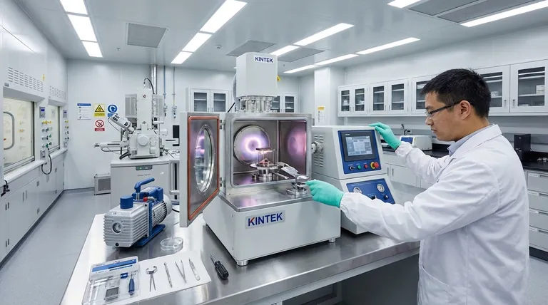
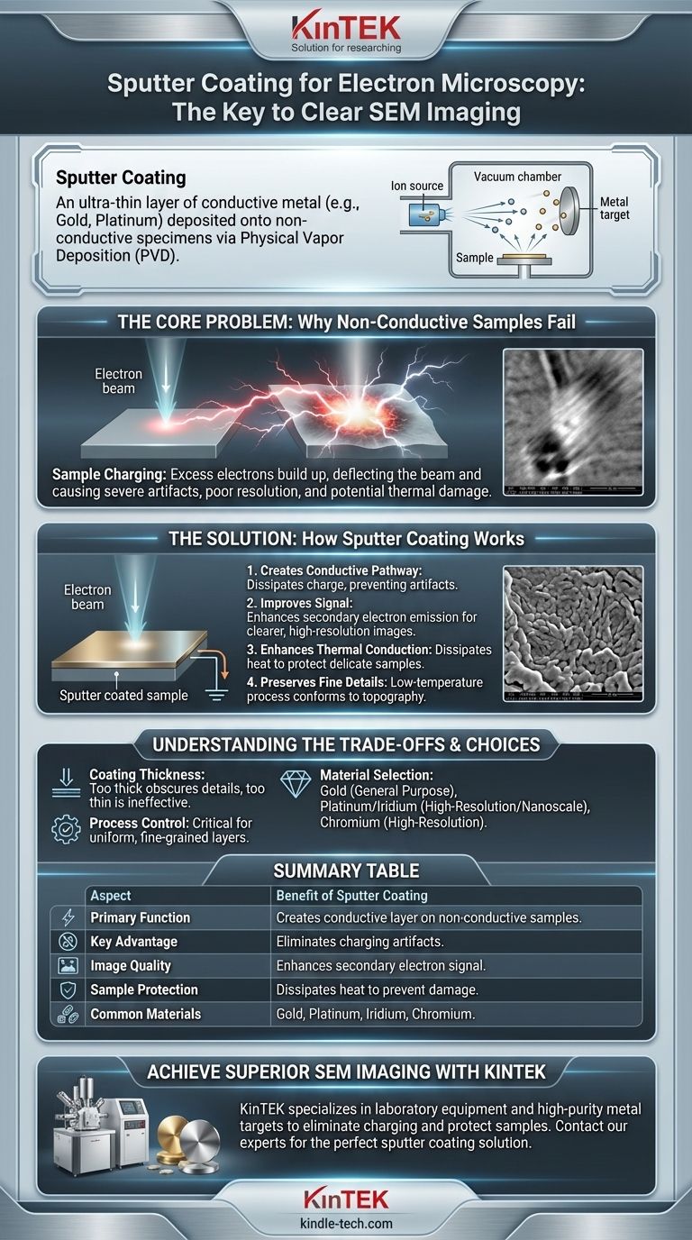
In the context of electron microscopy, sputter coating is a preparatory technique where an ultra-thin layer of electrically conductive material, typically a metal like gold or platinum, is deposited onto a non-conductive specimen. This process, a form of Physical Vapor Deposition (PVD), involves bombarding a metal target with high-energy ions in a vacuum, which dislodges metal atoms that then evenly coat the sample's surface.
The fundamental challenge in Scanning Electron Microscopy (SEM) is that non-conductive samples accumulate electrical charge from the electron beam, severely distorting the image. Sputter coating is the definitive solution, rendering the specimen's surface conductive to dissipate this charge and enable clear, high-resolution imaging.
The Core Problem: Why Non-Conductive Samples Fail in SEM
To understand the necessity of sputter coating, we must first examine the problem it solves. An SEM creates an image by scanning a surface with a focused beam of electrons.
The Issue of "Charging"
When the electron beam hits a conductive sample, the excess electrons have a path to ground. However, on non-conductive materials like polymers, ceramics, or biological tissue, these electrons accumulate on the surface.
This phenomenon is known as sample charging.
The Impact on Image Quality
This trapped electrical charge deflects the incoming electron beam and interferes with the signals used to form the image. This results in severe imaging artifacts, such as bright patches, streaks, and a dramatic loss of detail and resolution.
Without a conductive surface, obtaining a useful image from most non-metallic samples is nearly impossible.
The Risk of Sample Damage
The energy from the electron beam can also build up as localized heat. For delicate or heat-sensitive specimens, this can cause melting, distortion, or other forms of beam-induced damage, destroying the very features you intend to study.
How Sputter Coating Provides the Solution
Sputter coating directly counteracts the issues of charging and beam damage by fundamentally altering the sample's surface properties.
Creating a Conductive Pathway
The primary benefit is creating a path to ground. The thin, continuous metal film allows the excess charge from the electron beam to flow away from the imaged area, completely preventing charging artifacts.
Improving Signal for Better Images
The metallic coating significantly improves the emission of secondary electrons—the primary signal used to generate the high-resolution topographical images SEM is known for. This results in a much stronger, clearer signal and a crisper final image.
Enhancing Thermal Conduction
The metal layer is also an excellent thermal conductor. It effectively dissipates heat away from the point of contact with the electron beam, protecting delicate samples from thermal damage.
Preserving Fine Surface Details
Because sputtering is a low-temperature process, it is perfectly suited for heat-sensitive materials like biological samples. It deposits a coating that conforms precisely to the sample's existing topography, preserving even intricate, three-dimensional surfaces for accurate imaging.
Understanding the Trade-offs
While essential, sputter coating is a process that requires precision. The goal is to replicate the sample's surface, not obscure it.
The Coating Is Not the Sample
It is critical to remember that you are ultimately imaging the metallic coating. A coating that is too thick can obscure fine surface details, while an uneven coating can introduce artifacts that do not exist on the original specimen.
Material Selection Matters
Different coating materials are used for different purposes.
- Gold is a common, effective choice for general-purpose work.
- Platinum or Iridium have a much finer grain structure and are used for very high-magnification work where nanoscale details must be preserved.
- Chromium can also be used and offers excellent properties for high-resolution applications.
Process Control is Crucial
The quality of the coating depends on factors like vacuum level, coating time, and current. A poorly controlled process can lead to large grain sizes or uneven layers, compromising image quality.
Making the Right Choice for Your Goal
Applying this understanding allows you to tailor your sample preparation to your specific analytical needs.
- If your primary focus is routine imaging of robust samples: A standard gold or gold/palladium coating provides an excellent balance of conductivity and image quality.
- If your primary focus is high-resolution imaging of fine surface details: An ultra-thin coating of a fine-grained material like platinum, iridium, or chromium is necessary to avoid obscuring nanoscale features.
- If your primary focus is analyzing heat-sensitive or biological specimens: Sputter coating is the ideal method, as its low-temperature nature protects the sample from thermal damage while eliminating charging.
Ultimately, sputter coating is the essential preparatory step that transforms an un-imageable specimen into a source of high-fidelity scientific data.
Summary Table:
| Aspect | Benefit of Sputter Coating |
|---|---|
| Primary Function | Creates a conductive layer on non-conductive samples |
| Key Advantage | Eliminates charging artifacts from the electron beam |
| Image Quality | Enhances secondary electron signal for clearer images |
| Sample Protection | Dissipates heat to prevent beam damage |
| Common Materials | Gold, Platinum, Iridium, Chromium |
Achieve Superior SEM Imaging with KINTEK
Are you struggling with charging artifacts or poor image quality from your non-conductive samples? KINTEK specializes in laboratory equipment and consumables, including sputter coaters and the high-purity metal targets you need for flawless sample preparation.
Our expertise ensures you can:
- Eliminate charging and obtain clear, high-resolution images.
- Protect delicate samples from beam-induced damage.
- Select the right coating material (like fine-grained Platinum for high-magnification work) for your specific application.
Let us help you transform your un-imageable specimens into reliable scientific data. Contact our experts today to discuss your lab's needs and find the perfect sputter coating solution.
Visual Guide
Related Products
- HFCVD Machine System Equipment for Drawing Die Nano-Diamond Coating
- Electron Beam Evaporation Coating Oxygen-Free Copper Crucible and Evaporation Boat
- 400-700nm Wavelength Anti Reflective AR Coating Glass
People Also Ask
- Why is Chemical Vapor Deposition (CVD) equipment uniquely suited for constructing hierarchical superhydrophobic structures?
- What is the full form of HFCVD? A Guide to Hot Filament Chemical Vapor Deposition
- How expensive is chemical vapor deposition? Understanding the True Cost of High-Performance Coating
- What types of substrates are used in CVD to facilitate graphene films? Optimize Graphene Growth with the Right Catalyst
- What is the chemical vapor deposition growth process? Build Superior Thin Films from the Atom Up


