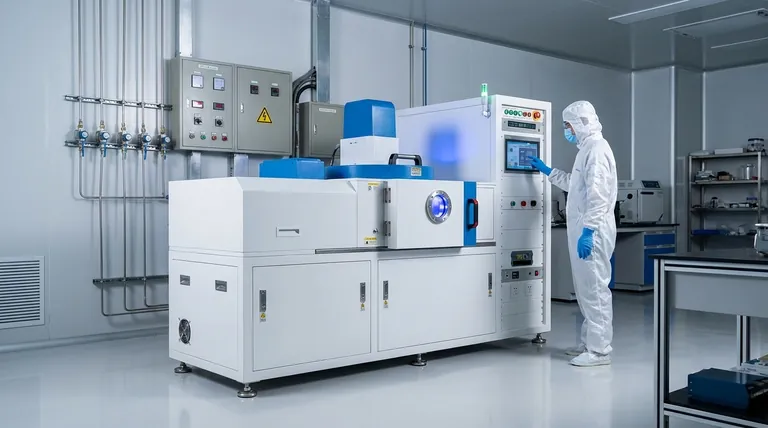
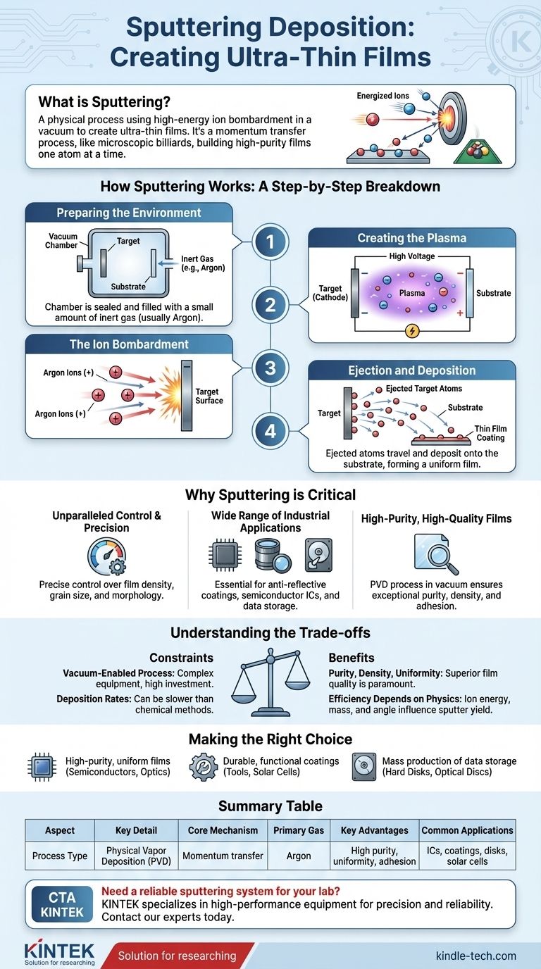
In the simplest terms, sputtering is a physical process used to create ultra-thin films of material. It works by bombarding a source material, known as a target, with high-energy ions inside a vacuum, which knocks atoms loose from the target and deposits them onto a substrate to form a coating.
Sputtering is fundamentally a momentum transfer process, akin to a microscopic game of billiards. By using energized gas ions as the "cue ball" to strike atoms on a target, it provides a highly controlled and versatile way to build high-purity films one atom at a time.
How Sputtering Works: A Step-by-Step Breakdown
To understand sputtering's value, we must first understand its core mechanics. The entire process takes place within a sealed vacuum chamber to ensure the purity and quality of the resulting film.
Step 1: Preparing the Environment
The process begins by placing both the substrate (the object to be coated) and the target (the source material for the coating) into a vacuum chamber. This chamber is then filled with a small amount of an inert gas, most commonly Argon.
Step 2: Creating the Plasma
A high voltage is applied between the target and the substrate, with the target acting as the negative electrode (cathode). This strong electric field energizes the chamber and strips electrons from the Argon atoms, creating a glowing, ionized gas known as a plasma.
Step 3: The Ion Bombardment
The positively charged Argon ions created in the plasma are now forcefully accelerated toward the negatively charged target. They collide with the target's surface at extremely high velocities.
Step 4: Ejection and Deposition
This high-energy bombardment physically knocks atoms loose from the target material's surface. These ejected atoms travel through the vacuum chamber and land on the substrate, gradually building up to form a thin, uniform film.
Why Sputtering is a Critical Technology
Sputtering is not just a laboratory curiosity; it is a foundational technology in modern manufacturing. Its widespread use stems from the unique advantages it offers over other deposition methods.
Unparalleled Control and Precision
Sputtering allows for precise control over the final film's properties. By managing factors like gas pressure, voltage, and temperature, engineers can finely tune the film's density, grain size, and morphology, ensuring it meets exact specifications.
Wide Range of Industrial Applications
The versatility of sputtering is evident in its applications across numerous industries. It is essential for creating anti-reflective coatings on glass, depositing the metallic layers on computer hard disks and DVDs, and processing integrated circuits in the semiconductor industry.
High-Purity, High-Quality Films
Because sputtering is a physical vapor deposition (PVD) process that occurs in a vacuum, it avoids the chemical reactions and contaminants common in other methods. This results in exceptionally pure and dense coatings with strong adhesion to the substrate.
Understanding the Trade-offs
While powerful, sputtering is a specific tool chosen for its distinct benefits. Understanding its operational constraints is key to appreciating its role.
It is a Vacuum-Enabled Process
The requirement for a high-vacuum environment means that sputtering equipment is complex and represents a significant capital investment. The process cannot be performed in an open-air environment.
Deposition Rates Can Be a Factor
Compared to some chemical deposition methods, sputtering can be a slower process. The trade-off is typically speed versus quality; sputtering is chosen when the purity, density, and uniformity of the film are more critical than the raw speed of deposition.
Efficiency Depends on Physics
The effectiveness of the process is governed by the laws of physics. The energy, mass, and angle of the bombarding ions, as well as the binding energy of the target atoms, all influence the "sputter yield"—the number of atoms ejected per incoming ion.
Making the Right Choice for Your Goal
Selecting a deposition method depends entirely on the desired outcome. Sputtering excels in scenarios where precision and quality are paramount.
- If your primary focus is high-purity, uniform films: Sputtering is the industry standard for applications like semiconductors and optical components where film quality is non-negotiable.
- If your primary focus is durable, functional coatings: This method is a leading choice for creating wear-resistant tool coatings, decorative finishes, and conductive layers on solar cells.
- If your primary focus is mass production of data storage media: The reliability and precision of sputtering make it the foundational technology for manufacturing computer hard disks and optical discs.
Ultimately, sputtering empowers us to engineer materials at the atomic level, building the high-performance surfaces that drive modern technology.
Summary Table:
| Aspect | Key Detail |
|---|---|
| Process Type | Physical Vapor Deposition (PVD) |
| Core Mechanism | Momentum transfer from ion bombardment |
| Primary Gas Used | Argon |
| Key Advantages | High film purity, excellent uniformity, strong adhesion |
| Common Applications | Semiconductor ICs, optical coatings, hard disks, solar cells |
Need a reliable sputtering system for your lab's thin film research or production?
KINTEK specializes in high-performance lab equipment, including sputtering deposition systems designed for precision and reliability. Whether you are developing semiconductor devices, optical coatings, or advanced materials, our solutions ensure the high-purity, uniform films critical to your success.
Contact our experts today to discuss your specific requirements and discover how KINTEK's sputtering technology can enhance your laboratory's capabilities.
Visual Guide
Related Products
- Chemical Vapor Deposition CVD Equipment System Chamber Slide PECVD Tube Furnace with Liquid Gasifier PECVD Machine
- Customer Made Versatile CVD Tube Furnace Chemical Vapor Deposition Chamber System Equipment
- HFCVD Machine System Equipment for Drawing Die Nano-Diamond Coating
- RF PECVD System Radio Frequency Plasma-Enhanced Chemical Vapor Deposition RF PECVD
- 915MHz MPCVD Diamond Machine Microwave Plasma Chemical Vapor Deposition System Reactor
People Also Ask
- What types of substrates are used in CVD to facilitate graphene films? Optimize Graphene Growth with the Right Catalyst
- What happens during deposition chemistry? Building Thin Films from Gaseous Precursors
- What are the advantages of chemical vapor deposition? Achieve Superior Thin Films for Your Lab
- What is plasma enhanced chemical vapor deposition PECVD equipment? A Guide to Low-Temperature Thin Film Deposition
- How are carbon nanotubes grown? Master Scalable Production with Chemical Vapor Deposition


