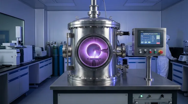
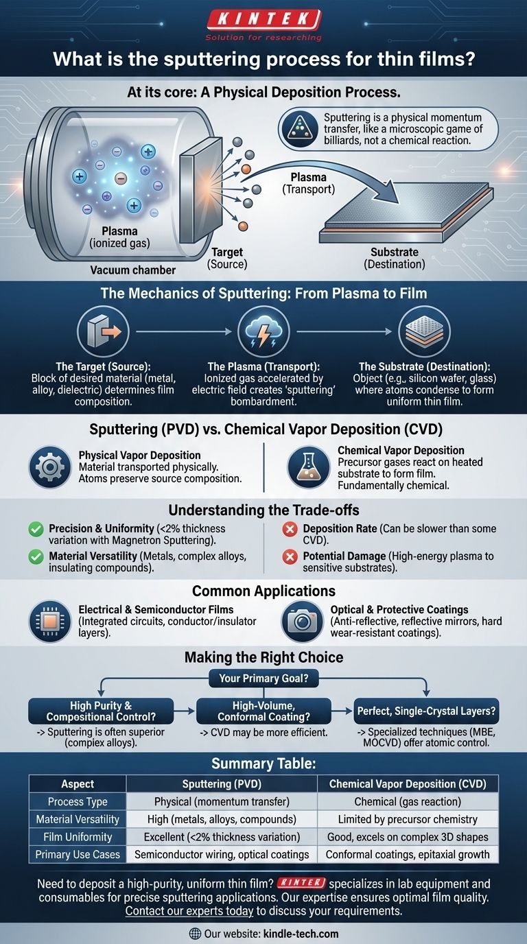
At its core, sputtering is a physical deposition process used to create ultra-thin layers of material, often just atoms thick. In a vacuum, energetic ions from a plasma are accelerated to strike a source material, called a target. This collision physically knocks atoms loose from the target, which then travel and deposit onto a substrate, gradually building up the desired thin film.
Sputtering is not a chemical reaction but a physical momentum transfer, like a microscopic game of billiards. This distinction makes it an exceptionally precise and versatile technique for depositing a wide range of pure materials and complex alloys that are difficult or impossible to create with chemical methods.
The Mechanics of Sputtering: From Plasma to Film
To understand sputtering, it's best to break it down into its three fundamental components: the source, the transport process, and the substrate.
The Target (The Source)
The target is a block of the exact material you want to deposit. This can be a pure metal, an alloy, or a dielectric compound. The composition of the target directly determines the composition of the final film.
The Plasma (The Transport)
A plasma—an ionized gas—is created inside the vacuum chamber. An electric field accelerates these ions, sending them crashing into the target with significant force. This bombardment is the "sputtering" event that ejects atoms from the target's surface.
The Substrate (The Destination)
The substrate is the object onto which the film is grown, such as a silicon wafer, a piece of glass, or a medical implant. The ejected target atoms travel through the vacuum and condense on the substrate's surface, forming a uniform, thin film.
Sputtering in Context: Physical vs. Chemical Deposition
Thin film deposition methods fall into two major categories. Understanding this distinction is key to knowing when and why to use sputtering.
Physical Vapor Deposition (PVD)
Sputtering is a form of Physical Vapor Deposition (PVD). PVD methods physically transport material from a source to the substrate without intended chemical reactions. Other PVD techniques include thermal evaporation and electron beam evaporation.
The key characteristic of PVD is that the material arrives at the substrate in an atomic or molecular form, preserving the source's basic composition.
Chemical Vapor Deposition (CVD)
In contrast, Chemical Vapor Deposition (CVD) involves introducing precursor gases into a reactor. These gases decompose and react on the heated substrate surface to form the desired film.
For example, silane gas (SiH4) is used in CVD to deposit a solid silicon (Si) film. The process is fundamentally chemical, relying on specific reactions to create the final material.
Understanding the Trade-offs of Sputtering
No single technique is perfect for every scenario. Sputtering has clear advantages but also inherent limitations.
Advantage: Precision and Uniformity
Modern magnetron sputtering systems offer exceptional control over film thickness. It is common to achieve less than 2% thickness variation across an entire substrate, which is critical for semiconductor devices and optical coatings.
Advantage: Material Versatility
Because it is a physical process, sputtering can deposit nearly any material that can be made into a target. This includes pure metals, complex multi-element alloys, and insulating compounds, which are often challenging for chemical methods.
Potential Limitation: Deposition Rate and Damage
Sputtering can be slower than some high-rate CVD processes, making it less ideal for applications requiring very thick films. Additionally, the high-energy plasma environment can sometimes cause damage to extremely sensitive substrates or electronic devices.
Common Applications for Sputtered Films
The precision and versatility of sputtering make it a cornerstone technology in numerous high-tech industries.
Electrical and Semiconductor Films
Sputtering is essential for manufacturing integrated circuits. It is used to deposit the microscopic layers of conductors (like copper or aluminum) and insulators that form the wiring and components of a microchip.
Optical and Protective Coatings
The process is widely used to apply anti-reflective coatings on lenses and screens, reflective layers on mirrors, and coatings for solar cells. It is also used to create extremely hard, wear-resistant coatings on cutting tools and machine parts.
Making the Right Choice for Your Goal
Selecting a deposition method requires aligning the technique's strengths with your project's primary objective.
- If your primary focus is high purity and compositional control: Sputtering is often the superior choice, especially for depositing complex metal alloys where stoichiometry is critical.
- If your primary focus is high-volume, conformal coating of complex 3D shapes: A method like Chemical Vapor Deposition (CVD) may be more efficient due to the nature of gas-phase transport.
- If your primary focus is creating perfect, single-crystal layers: Highly specialized techniques like Molecular Beam Epitaxy (MBE) or Metalorganic CVD (MOCVD) offer unparalleled atomic-level control.
Understanding the fundamental mechanism of each deposition technique empowers you to select the optimal process for your specific material and application.
Summary Table:
| Aspect | Sputtering (PVD) | Chemical Vapor Deposition (CVD) |
|---|---|---|
| Process Type | Physical (momentum transfer) | Chemical (gas reaction) |
| Material Versatility | High (metals, alloys, compounds) | Limited by precursor chemistry |
| Film Uniformity | Excellent (<2% thickness variation) | Good, excels on complex 3D shapes |
| Primary Use Cases | Semiconductor wiring, optical coatings | Conformal coatings, epitaxial growth |
Need to deposit a high-purity, uniform thin film? KINTEK specializes in lab equipment and consumables for precise sputtering applications. Our expertise ensures you achieve optimal film quality for semiconductors, optics, and protective coatings. Contact our experts today to discuss your specific deposition requirements and find the right solution for your laboratory.
Visual Guide
Related Products
- HFCVD Machine System Equipment for Drawing Die Nano-Diamond Coating
- 915MHz MPCVD Diamond Machine Microwave Plasma Chemical Vapor Deposition System Reactor
- Laboratory Sterilizer Lab Autoclave Pulse Vacuum Lifting Sterilizer
- Vacuum Hot Press Furnace Machine for Lamination and Heating
- Laboratory Sterilizer Lab Autoclave Vertical Pressure Steam Sterilizer for Liquid Crystal Display Automatic Type
People Also Ask
- How do CVD diamonds grow? A Step-by-Step Guide to Lab-Grown Diamond Creation
- What is the hot filament chemical vapour deposition of diamond? A Guide to Synthetic Diamond Coating
- How do you calculate coating coverage? A Practical Guide to Accurate Material Estimation
- How is diamond coating made? A Guide to CVD and PVD Methods
- What is the process of coating deposition? A Step-by-Step Guide to Thin Film Engineering


