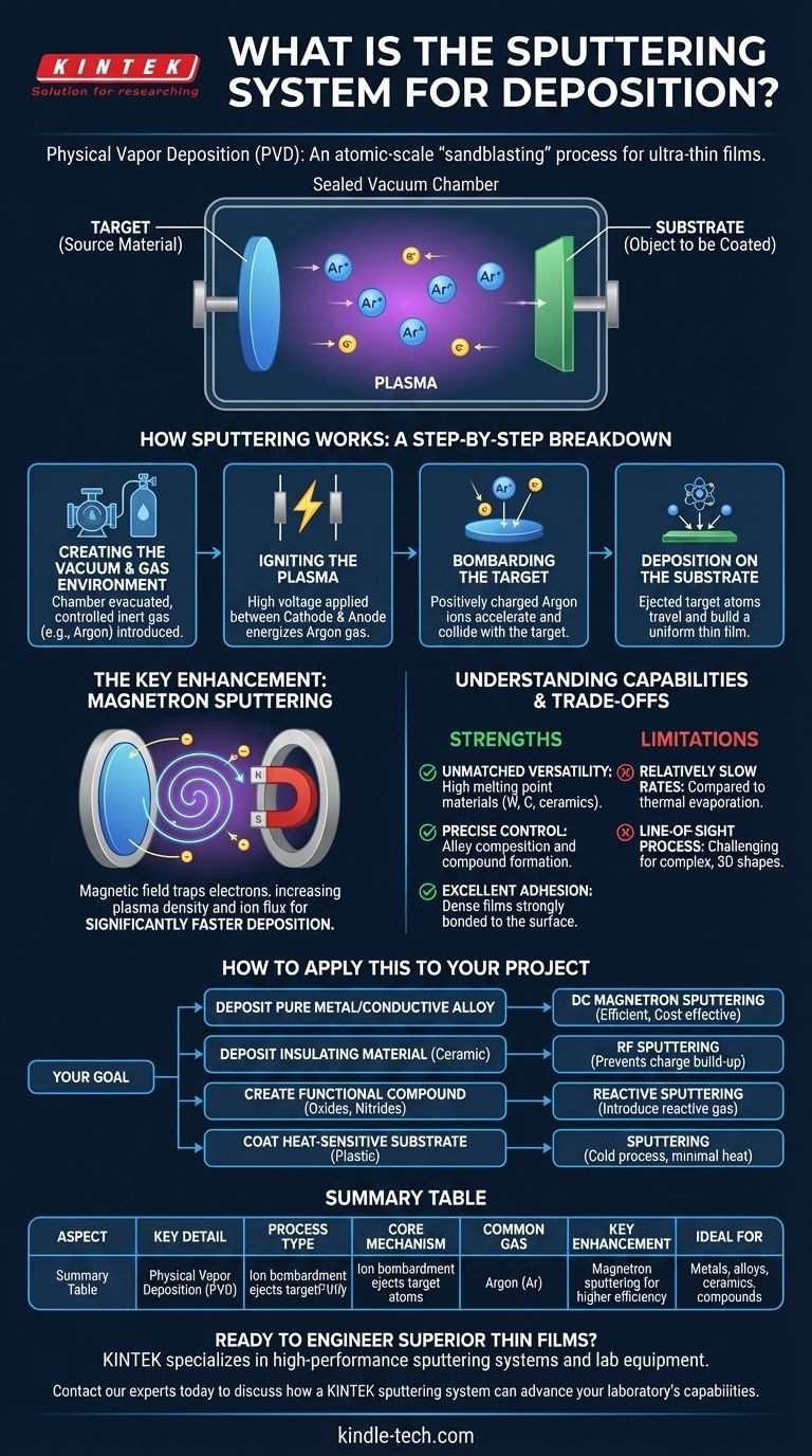
At its core, a sputtering system is a machine that deposits ultra-thin films of material onto a surface within a vacuum. It operates by physically ejecting atoms from a source material (the "target") using high-energy ion bombardment, which then travel and coat a desired object (the "substrate"). This process is a highly controlled form of physical vapor deposition (PVD).
Sputtering should not be thought of as melting or evaporation. It is an atomic-scale "sandblasting" process where ions act as the grit, chipping atoms off a target. This physical mechanism gives it remarkable versatility and control over the final film's properties.

How Sputtering Works: A Step-by-Step Breakdown
Sputtering deposition is a precise, multi-step process that takes place entirely within a sealed vacuum chamber. The core principle is the transfer of momentum from an energetic ion to the atoms of the target material.
Step 1: Creating the Vacuum and Gas Environment
First, the chamber is evacuated to a high vacuum to remove any contaminants. Then, a small, controlled amount of an inert gas—most commonly argon (Ar)—is introduced. This gas provides the ions necessary for the process.
Step 2: Igniting the Plasma
A high voltage is applied between two electrodes: the cathode, which holds the target material, and the anode, which holds the substrate to be coated. This strong electric field energizes the argon gas, stripping electrons from the argon atoms and creating a plasma—a glowing, ionized gas consisting of positive argon ions (Ar+) and free electrons.
Step 3: Bombarding the Target
The positively charged argon ions are forcefully accelerated by the electric field toward the negatively charged target (the cathode). They collide with the target surface with significant energy, typically many times the bond energy holding the target's atoms together.
Step 4: Deposition on the Substrate
This high-energy impact physically knocks out, or "sputters," atoms from the target material. These ejected atoms travel through the vacuum chamber and land on the substrate, gradually building up a thin, uniform film.
The Key Enhancement: Magnetron Sputtering
While basic sputtering works, it is often slow. Most modern systems use magnetron sputtering to dramatically increase deposition rates and efficiency.
The Role of the Magnetic Field
In a magnetron system, strong magnets are placed behind the target. This magnetic field traps the free electrons from the plasma in a spiral path directly in front of the target surface.
Why This Matters: Higher Efficiency
These trapped electrons are forced to travel a much longer path, massively increasing their chances of colliding with and ionizing more argon atoms. This creates a much denser plasma, a higher flux of ions bombarding the target, and ultimately, a significantly faster deposition rate.
Understanding the Capabilities and Trade-offs
Sputtering is a powerful technique, but like any process, it has specific strengths and limitations that make it suitable for certain applications.
Strength: Unmatched Material Versatility
Because sputtering is a physical rather than a thermal process, it can deposit materials with extremely high melting points, such as tungsten, carbon, and ceramics, which are difficult or impossible to deposit using thermal evaporation.
Strength: Precise Alloy and Compound Control
Sputtering allows for the deposition of alloys with a precise composition that is maintained from the target to the substrate. Furthermore, by introducing a reactive gas like oxygen or nitrogen into the chamber, one can create compound films like oxides and nitrides directly on the substrate—a technique known as reactive sputtering.
Strength: Excellent Adhesion and Film Density
The sputtered atoms arrive at the substrate with considerable kinetic energy, which results in films that are very dense and strongly adhered to the surface.
Limitation: Relatively Slow Deposition Rates
Even with magnetron enhancement, sputtering is generally a slower process compared to thermal evaporation, which can be a factor in high-volume manufacturing.
Limitation: Line-of-Sight Process
Sputtered atoms travel in relatively straight lines. This can make it challenging to achieve a perfectly uniform coating on complex, three-dimensional shapes without sophisticated substrate rotation.
How to Apply This to Your Project
Your choice of sputtering technique depends entirely on the material you need to deposit and the properties you want to achieve.
- If your primary focus is depositing a pure metal or conductive alloy: DC magnetron sputtering is the standard, most efficient, and cost-effective method.
- If your primary focus is depositing an insulating material like a ceramic: RF sputtering is required, as it uses an alternating current to prevent charge from building up on the non-conductive target surface.
- If your primary focus is creating a functional compound (e.g., a hard coating or an optical filter): Reactive sputtering is the ideal technique for forming precise oxides, nitrides, or carbides.
- If your primary focus is coating a heat-sensitive substrate like plastic: Sputtering is an excellent choice as it is a "cold" process that imparts minimal heat to the substrate.
By understanding these core principles, you can leverage sputtering to engineer high-performance thin films for nearly any advanced application.
Summary Table:
| Aspect | Key Detail |
|---|---|
| Process Type | Physical Vapor Deposition (PVD) |
| Core Mechanism | Ion bombardment ejects target atoms |
| Common Gas | Argon (Ar) |
| Key Enhancement | Magnetron sputtering for higher efficiency |
| Ideal For | Metals, alloys, ceramics, compounds |
Ready to engineer superior thin films for your research or production?
KINTEK specializes in high-performance sputtering systems and lab equipment. Whether you need to deposit conductive metals with DC magnetron sputtering, insulators with RF sputtering, or create custom compounds with reactive sputtering, our solutions deliver precise control, excellent adhesion, and unmatched material versatility.
Contact our experts today to discuss how a KINTEK sputtering system can advance your laboratory's capabilities.
Visual Guide
Related Products
- Spark Plasma Sintering Furnace SPS Furnace
- Vacuum Induction Melting Spinning System Arc Melting Furnace
- Chemical Vapor Deposition CVD Equipment System Chamber Slide PECVD Tube Furnace with Liquid Gasifier PECVD Machine
- Customer Made Versatile CVD Tube Furnace Chemical Vapor Deposition Chamber System Equipment
People Also Ask
- What is the mechanism of SPS process? A Deep Dive into Rapid, Low-Temperature Sintering
- What are the advantages of CAMI/SPS for W-Cu composite preparation? Reduce cycles from hours to seconds.
- What is the difference between spark plasma sintering and flash sintering? A Guide to Advanced Sintering Methods
- Why are Spark Plasma Sintering (SPS) furnaces or hot presses utilized in the preparation of Li3PS4 solid electrolytes?
- What is the process fundamentals of spark plasma sintering? Achieve Rapid, High-Density Material Consolidation


