In essence, thin film deposition is the process of applying an extremely thin layer of material, often just a few atoms or molecules thick, onto a surface or "substrate." This technology is the foundational manufacturing method for a vast range of modern high-tech components, from computer chips to solar panels. It allows us to precisely engineer the properties of a surface by adding a new material with desired mechanical, electrical, or optical characteristics.
The core concept to grasp is that "thin film deposition" is not a single technique, but a family of highly controlled processes. These processes fall into two main categories—physical and chemical—each with distinct methods designed to build functional, microscopic layers that are essential for virtually all modern electronics.

Why This Technology is Foundational
Thin film deposition isn't an obscure industrial process; it is a critical enabler of the technology we use every day. Its ability to create materials with novel properties makes it indispensable.
The Impact on Electronics and Semiconductors
Nearly every integrated circuit and semiconductor device is built using these techniques. Deposition is used to create the conductive, insulating, and semiconducting layers that form transistors and connectors on a silicon wafer.
Applications Beyond Computing
The technology's benefits extend far beyond microchips. It is used to create anti-reflective coatings on eyeglasses, durable and decorative finishes on tools, conductive layers in solar panels, and the magnetic layers on hard disk drives.
Pushing the Boundaries of Nanotechnology
By allowing for the manipulation of materials at the atomic level, thin film deposition is a cornerstone of nanotechnology. It enables the creation of materials with super-hard, corrosion-resistant, or specific photosensitive properties.
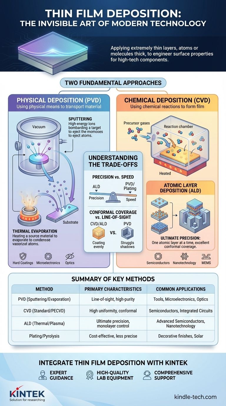
The Two Fundamental Approaches
All deposition methods can be broadly categorized by how they transport the coating material to the substrate. The choice between them depends entirely on the material being used and the desired properties of the final film.
Physical Deposition
This approach uses physical means—such as heat or kinetic energy—to transform a solid source material into a vapor. These vaporized atoms or molecules then travel through a vacuum and condense onto the cooler substrate, forming the thin film.
Chemical Deposition
This approach uses chemical reactions to form the film. Precursor gases are introduced into a reaction chamber where they react or decompose on the substrate's surface, leaving behind the desired solid material as a thin coating.
Key Deposition Techniques Explained
Within the two fundamental approaches, several specific methods have become industry standards. Each offers a unique combination of precision, speed, and material compatibility.
Physical Vapor Deposition (PVD)
PVD is a general term for methods that physically transfer material. The most common techniques are sputtering, where high-energy ions bombard a source to eject atoms, and thermal evaporation, where the source material is heated in a vacuum until it evaporates.
Chemical Vapor Deposition (CVD)
CVD is the most widely used method in the semiconductor industry. Its reliance on controlled chemical reactions allows for highly uniform and precise coatings, which is essential for manufacturing complex integrated circuits.
Atomic Layer Deposition (ALD)
A more advanced subset of chemical deposition, ALD builds the film one single atomic layer at a time. It uses a sequence of self-limiting chemical reactions, offering unparalleled control over film thickness and conformity, even on complex 3D structures.
Plating and Pyrolysis
Other methods also exist. Plating involves submerging the substrate in a chemical bath where the coating material adheres to the surface. Spray pyrolysis involves spraying a chemical solution onto a heated substrate, where it thermally decomposes to form the film.
Understanding the Trade-offs
No single deposition method is universally superior. The selection of a technique is a critical engineering decision based on a series of trade-offs between cost, speed, and the desired outcome.
Precision vs. Speed
Methods like ALD offer the ultimate precision, but this layer-by-layer approach is inherently slow. In contrast, techniques like sputtering (PVD) or plating can deposit material much more quickly but may offer less control over atomic-level uniformity.
Material and Substrate Compatibility
CVD often requires high temperatures, which can damage sensitive substrates. PVD can typically be performed at lower temperatures, making it suitable for a wider range of materials, including plastics.
Conformal Coverage vs. Line-of-Sight
PVD is often a "line-of-sight" process, meaning it struggles to evenly coat complex, three-dimensional shapes with undercuts. Chemical methods like CVD and especially ALD excel at creating highly conformal coatings that uniformly cover every exposed surface of a complex object.
Matching the Method to Your Goal
To select the right process, you must first define your most critical requirement.
- If your primary focus is ultimate precision and conformity for complex 3D nanostructures: ALD is the leading choice due to its atomic-level, layer-by-layer control.
- If your primary focus is high-throughput semiconductor manufacturing: CVD is the industry standard for its excellent balance of high precision, uniformity, and efficiency.
- If your primary focus is creating high-purity metallic or ceramic hard coatings: PVD techniques like sputtering are highly effective and widely used for applications from tools to optics.
- If your primary focus is cost-effective coating of larger objects without extreme precision: Simpler methods like electroplating or spray pyrolysis may be the most practical solution.
Ultimately, thin film deposition is the invisible art of building advanced materials from the atom up, enabling the performance and function of nearly every piece of modern technology.
Summary Table:
| Category | Key Methods | Primary Characteristics | Common Applications |
|---|---|---|---|
| Physical Vapor Deposition (PVD) | Sputtering, Thermal Evaporation | Line-of-sight, high-purity coatings, lower temperatures | Hard coatings for tools, microelectronics, optics |
| Chemical Vapor Deposition (CVD) | Standard CVD, Plasma-Enhanced CVD (PECVD) | High uniformity, conformal coatings, often requires high temperatures | Semiconductor manufacturing, integrated circuits |
| Atomic Layer Deposition (ALD) | Thermal ALD, Plasma-Enhanced ALD | Ultimate precision, monolayer control, excellent conformity on 3D structures | Advanced semiconductors, nanotechnology, MEMS |
| Other Methods | Plating, Spray Pyrolysis | Cost-effective for larger scales, less precise | Decorative finishes, some solar cell layers |
Ready to Integrate Thin Film Deposition into Your Workflow?
Choosing the right deposition technology is critical for the success of your R&D or manufacturing process. The experts at KINTEK are here to help you navigate these complex decisions.
We provide:
- Expert Guidance: Our team will help you select the ideal PVD, CVD, or ALD system based on your specific material, substrate, and performance requirements.
- High-Quality Lab Equipment: From research-grade systems to production-scale solutions, KINTEK supplies reliable equipment for precise and consistent thin film deposition.
- Comprehensive Consumables & Support: Ensure optimal performance with our range of high-purity target materials, source chemicals, and dedicated technical support.
Whether you are developing next-generation semiconductors, advanced optical coatings, or novel nanomaterials, KINTEK has the expertise and equipment to support your laboratory's thin film needs.
Contact our experts today for a personalized consultation and discover how our solutions can accelerate your innovation.
Visual Guide
Related Products
- Aluminized Ceramic Evaporation Boat for Thin Film Deposition
- Tungsten Evaporation Boat for Thin Film Deposition
- Electron Beam Evaporation Coating Oxygen-Free Copper Crucible and Evaporation Boat
- Molybdenum Tungsten Tantalum Evaporation Boat for High Temperature Applications
- Vacuum Hot Press Furnace Machine for Lamination and Heating
People Also Ask
- Why are high-purity ceramic boats used for lignin activation? Ensure Purity & Thermal Stability
- Why is an alumina boat selected for catalyst precursors? Ensure Sample Purity at 1000 °C
- What are the alternatives to sputtering? Choose the Right Thin Film Deposition Method
- What is thin film deposition? Unlock Advanced Surface Engineering for Your Materials
- Why is an alumina boat and Ti3AlC2 powder bed necessary for Ti2AlC sintering? Protect MAX Phase Purity


