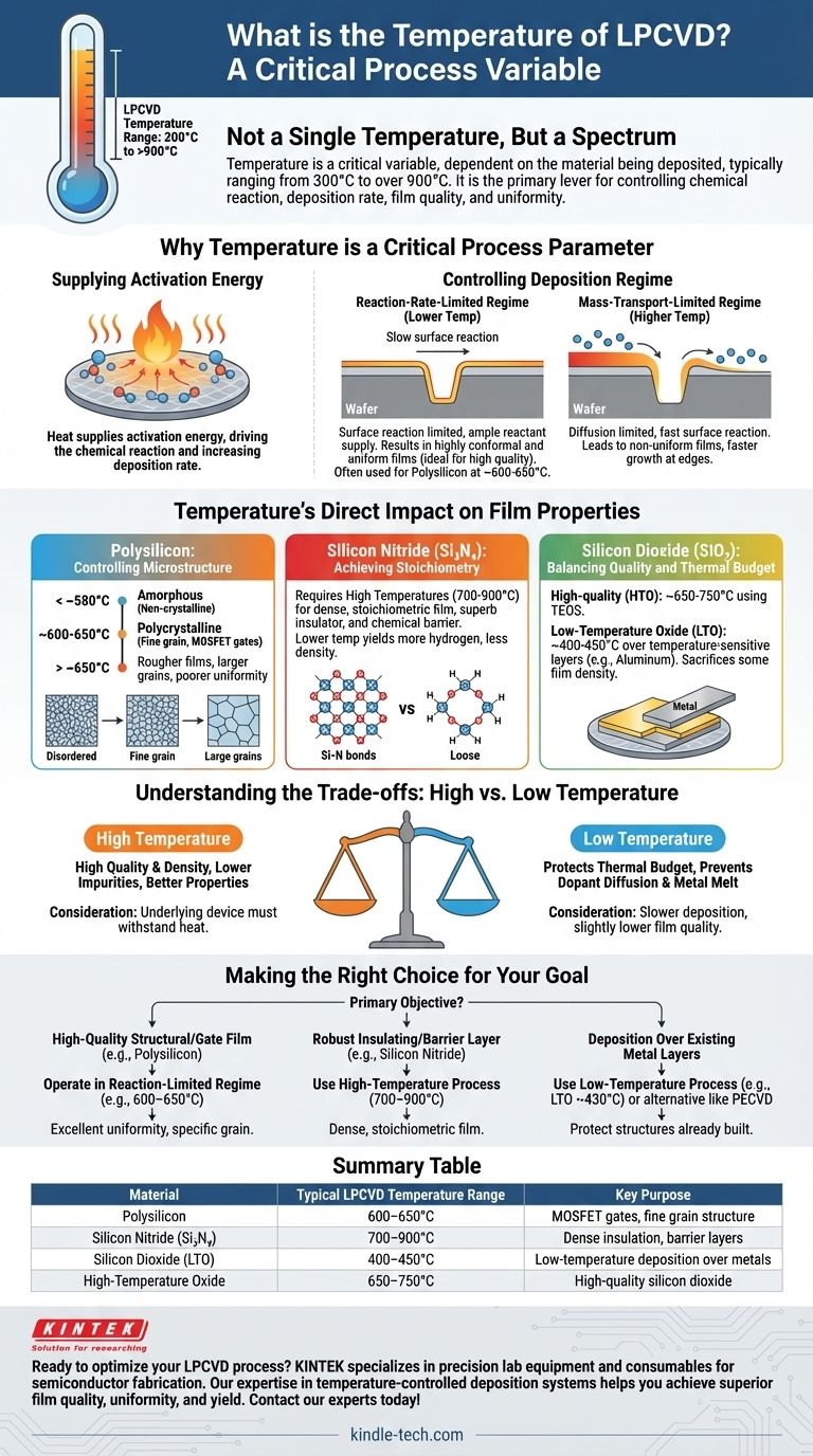
In Low-Pressure Chemical Vapor Deposition (LPCVD), there is no single temperature. Instead, temperature is a critical process variable set within a wide range—typically from 300°C to over 900°C—depending entirely on the specific material being deposited. For instance, polysilicon is commonly deposited around 600-650°C, while silicon nitride requires a much higher temperature of 700-900°C.
The temperature in LPCVD is deliberately chosen based on the specific material being deposited and the desired film properties. It is the primary lever for controlling the chemical reaction, directly influencing deposition rate, film quality, and uniformity across the wafer.
Why Temperature is a Critical Process Parameter
To truly understand LPCVD, one must see temperature not as a simple setting, but as the engine driving the entire deposition process. Its role is fundamental to the chemistry and physics of thin-film growth.
Supplying the Activation Energy
Every chemical reaction needs a certain amount of energy to get started, known as activation energy. In LPCVD, this energy is supplied by heat.
Increasing the temperature provides more thermal energy to the reactant gas molecules on the wafer surface, dramatically increasing the rate at which they react to form the solid film.
Controlling the Deposition Regime
The deposition rate in LPCVD is governed by one of two distinct regimes, and temperature is what determines which regime you are in.
-
Reaction-Rate-Limited Regime: At lower temperatures, the deposition rate is limited by the speed of the chemical reaction itself. There are plenty of reactant molecules available on the surface, but they lack the thermal energy to react quickly.
-
Mass-Transport-Limited Regime: At higher temperatures, the surface reaction is extremely fast. The deposition rate is now limited by how quickly fresh reactant gas molecules can travel (diffuse) through the gas to the wafer surface.
The Importance of the Reaction-Limited Regime
For high-quality films, LPCVD processes are almost always designed to operate in the reaction-rate-limited regime.
Because the reaction is the "slow step," reactant gases have ample time to diffuse and coat all surfaces of the wafer topography evenly. This results in a highly conformal and uniform film, which is a key advantage of LPCVD.
Operating in the mass-transport-limited regime leads to non-uniformity, as the film grows faster where the gas supply is more plentiful (e.g., the wafer's edge) and slower where it is depleted.
Temperature's Direct Impact on Film Properties
The chosen temperature directly dictates the final material properties of the deposited film. Different materials have unique requirements.
Polysilicon: Controlling Microstructure
For polysilicon, temperature determines the film's grain structure.
- Below ~580°C: The film deposits as amorphous (non-crystalline).
- Between ~600°C and 650°C: The film deposits as polycrystalline, with a fine grain structure ideal for many electronic applications like MOSFET gates.
- Above ~650°C: The surface reaction becomes too fast, leading to rougher films with larger grains and poorer uniformity.
Silicon Nitride (Si₃N₄): Achieving Stoichiometry
Stoichiometric silicon nitride (a precise Si₃N₄ ratio) is a superb insulator and chemical barrier.
Achieving this dense, high-quality film requires high temperatures, typically between 700°C and 900°C. Lower-temperature nitride films often contain more hydrogen, making them less dense and less effective as a barrier.
Silicon Dioxide (SiO₂): Balancing Quality and Thermal Budget
High-quality silicon dioxide can be deposited using a TEOS precursor at around 650°C to 750°C.
However, if the deposition needs to happen over temperature-sensitive layers (like aluminum), a "Low-Temperature Oxide" (LTO) process is used. This process runs at a much lower ~400-450°C, sacrificing some film density for a lower thermal budget.
Understanding the Trade-offs: High vs. Low Temperature
The choice of temperature is always a balance between achieving the ideal film properties and respecting the limitations of the overall device fabrication process.
The Case for High Temperature
Higher temperatures generally lead to films with higher density, lower impurity levels (like hydrogen), and better structural or electrical properties. If the underlying device can withstand the heat, a higher temperature often yields a higher-quality film.
The Necessity of Low Temperature
A device's thermal budget is the total amount of heat it can endure throughout manufacturing. High-temperature steps can cause previously implanted dopants to diffuse, or melt metal layers.
Therefore, later deposition steps in a process flow often demand lower temperatures to protect the structures already built on the wafer. This can mean accepting a slower deposition rate or slightly lower film quality.
Making the Right Choice for Your Goal
The optimal LPCVD temperature is defined by your primary objective.
- If your primary focus is a high-quality structural or gate film (e.g., Polysilicon): Operate in the tightly controlled, reaction-limited regime (e.g., 600-650°C) to ensure excellent uniformity and specific grain structure.
- If your primary focus is a robust insulating or barrier layer (e.g., Silicon Nitride): Use a high-temperature process (700-900°C) to achieve a dense, stoichiometric film.
- If your primary focus is deposition over existing metal layers: You must use a dedicated low-temperature process (e.g., LTO at ~430°C) or switch to an alternative method like Plasma-Enhanced CVD (PECVD).
Mastering temperature control is the key to leveraging the full power and precision of the LPCVD process.
Summary Table:
| Material | Typical LPCVD Temperature Range | Key Purpose |
|---|---|---|
| Polysilicon | 600-650°C | MOSFET gates, fine grain structure |
| Silicon Nitride (Si₃N₄) | 700-900°C | Dense insulation, barrier layers |
| Silicon Dioxide (LTO) | 400-450°C | Low-temperature deposition over metals |
| High-Temperature Oxide | 650-750°C | High-quality silicon dioxide |
Ready to optimize your LPCVD process? KINTEK specializes in precision lab equipment and consumables for semiconductor fabrication. Our expertise in temperature-controlled deposition systems helps you achieve superior film quality, uniformity, and yield. Whether you're working with polysilicon, silicon nitride, or low-temperature oxides, we have the solutions to meet your specific thermal requirements. Contact our experts today to discuss how we can enhance your thin-film deposition capabilities!
Visual Guide
Related Products
- Inclined Rotary Plasma Enhanced Chemical Vapor Deposition PECVD Equipment Tube Furnace Machine
- Inclined Rotary Plasma Enhanced Chemical Vapor Deposition PECVD Equipment Tube Furnace Machine
- Chemical Vapor Deposition CVD Equipment System Chamber Slide PECVD Tube Furnace with Liquid Gasifier PECVD Machine
- Laboratory CVD Boron Doped Diamond Materials
- Microwave Plasma Chemical Vapor Deposition MPCVD Machine System Reactor for Lab and Diamond Growth
People Also Ask
- How does the PECVD function enhance thin-film properties? Achieve Superior Chemical Stability & Durability
- How does plasma enhance CVD? Unlock Low-Temperature, High-Quality Film Deposition
- What is the core value of PECVD compared to CVD? Discover the Low-Temperature Advantage for Thin-Film Coating
- What is plasma enhanced chemical vapor deposition PECVD equipment? A Guide to Low-Temperature Thin Film Deposition
- How does plasma vapor deposition work? A Low-Temperature Coating Solution for Sensitive Materials


