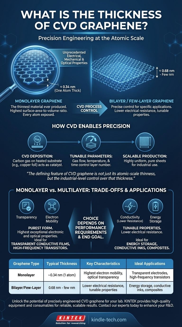
In its purest form, CVD graphene is a single layer of carbon atoms, making it the thinnest material ever produced at just one atom thick. The Chemical Vapor Deposition (CVD) method is prized for its ability to reliably produce these high-quality, single-layer sheets over large areas. The process also allows for precise control, enabling the intentional creation of bi-layer or few-layer graphene when specific applications demand it.
The defining feature of CVD graphene is not just its atomic-scale thinness, but the industrial-level control over that thickness. This precision is what allows its unique electrical, mechanical, and optical properties to be harnessed for specific, high-performance applications.

The Principle of Atomic Thinness
The concept of a material being only one atom thick is the foundation of graphene's revolutionary properties. This structure is what separates it from all other materials.
What "One Atom Thick" Truly Means
Graphene is composed of carbon atoms arranged in a two-dimensional honeycomb pattern. You can visualize it as a single atomic plane carefully extracted from a block of graphite.
This structure gives graphene the highest surface-area-to-volume ratio of any material known. Every single atom is exposed and able to interact with its environment.
Why This Unprecedented Thinness Matters
This unique structure is directly responsible for graphene's remarkable characteristics. It is the strongest, most conductive, and one of the most transparent materials ever discovered.
When integrated into other materials, such as polymers, it can create composites with dramatically enhanced strength, durability, and the ability to conduct heat or electricity.
How CVD Enables Precision Control
While other methods can produce graphene, CVD is considered the most promising technique for large-scale industrial use because it offers unparalleled control over the final product's quality and thickness.
The CVD Production Method
The CVD process involves depositing a carbon-containing gas onto a heated substrate, typically a metal foil like copper. The substrate acts as a catalyst, causing the carbon atoms to arrange themselves into the characteristic honeycomb lattice.
This method allows for the creation of graphene sheets that are highly uniform, pure, and cover large areas, making it suitable for industrial applications.
From Monolayer to Multilayer
CVD is considered one of the best methods for reliably producing high-quality monolayer graphene. This is the ideal for many advanced electronic and optical uses.
By carefully tuning the process parameters—such as gas flow, temperature, and time—engineers can control the number of layers deposited, creating bi-layer or few-layer graphene with consistent characteristics.
Understanding the Trade-offs: Single vs. Multi-Layer
The choice between single-layer and multi-layer graphene is not a matter of which is "better," but which is right for the job. Each configuration offers a different set of advantages.
The Purity of Monolayer Graphene
Single-layer graphene represents the material in its purest form. It exhibits the most exceptional electronic and optical properties.
This makes it the ideal choice for applications where high electron mobility and optical transparency are critical, such as in transparent conductive films for displays or high-frequency transistors.
The Practical Benefits of Few-Layer Graphene
Adding a controlled number of layers can be beneficial for other applications. For example, few-layer graphene can offer lower electrical resistance, making it better suited for certain energy storage devices or conductive inks.
However, as layers are added, other properties like transparency will decrease. The selection is always a balance based on the specific performance requirements.
The Importance of Overall Quality
Beyond the number of layers, the quality of the film is paramount. The CVD process excels at producing graphene with high homogeneity and purity.
Factors like fine grain structure and imperviousness are just as critical as thickness for ensuring reliable, high-performance results in any application.
Making the Right Choice for Your Application
The ideal thickness of CVD graphene is dictated entirely by your end goal. Understanding your primary objective will guide your material selection.
- If your primary focus is advanced electronics or optical transparency: You require high-quality, single-layer CVD graphene to leverage its superior electronic mobility and clarity.
- If your primary focus is energy storage or bulk conductivity: Controlled few-layer graphene might offer enhanced performance due to its lower sheet resistance and increased charge density.
- If your primary focus is creating stronger composite materials: The number of layers and its integration with the polymer matrix are key variables to tune for the desired strength, durability, or thermal properties.
Ultimately, the power of CVD is its ability to transform graphene from a theoretical concept into a precisely engineered and scalable material.
Summary Table:
| Graphene Type | Typical Thickness | Key Characteristics | Ideal Applications |
|---|---|---|---|
| Monolayer | ~0.34 nm (1 atom) | Highest electron mobility, optical transparency | Transparent electrodes, high-frequency transistors |
| Bilayer/Few-Layer | 0.68 nm - few nm | Lower electrical resistance, tunable properties | Energy storage, conductive inks, composites |
Unlock the potential of precisely engineered CVD graphene for your lab. Whether your project requires ultra-pure monolayer sheets for advanced electronics or tailored few-layer graphene for energy storage, KINTEK provides the high-quality lab equipment and consumables you need to achieve reliable, scalable results. Contact our experts today to discuss how our solutions can enhance your research and development.
Visual Guide
Related Products
- Carbon Graphite Plate Manufactured by Isostatic Pressing Method
- CVD Diamond for Thermal Management Applications
- Laboratory CVD Boron Doped Diamond Materials
- Custom CVD Diamond Coating for Lab Applications
- Vertical High Temperature Graphite Vacuum Graphitization Furnace
People Also Ask
- What is isostatic pressing? Achieve Uniform Density and Complex Shapes
- What is the difference between CIP and HIP? A Guide to Choosing the Right Process
- What products are made by isostatic pressing? Achieve Flawless, High-Performance Components
- Why Use an Isostatic or High-Precision Hydraulic Press for Li/LLZO/Li Batteries? Master Solid-State Interfaces
- What is the density of isostatic graphite? Unlock Superior Performance for Demanding Applications