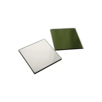
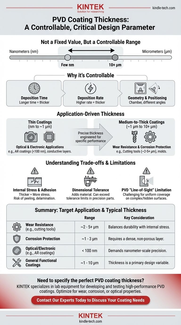
The thickness of a Physical Vapor Deposition (PVD) coating is not a single fixed value. Instead, it is a highly controllable parameter that typically ranges from a few nanometers (nm) to several micrometers (µm), or microns. The precise thickness is engineered based on the specific performance requirements of the application, such as wear resistance, corrosion protection, or desired optical properties.
The central takeaway is that PVD coating thickness is a critical design choice, not an inherent property. It involves a deliberate trade-off between enhancing a part's performance and managing factors like internal stress, dimensional tolerance, and manufacturing cost.
Why PVD Thickness is a Controllable Variable
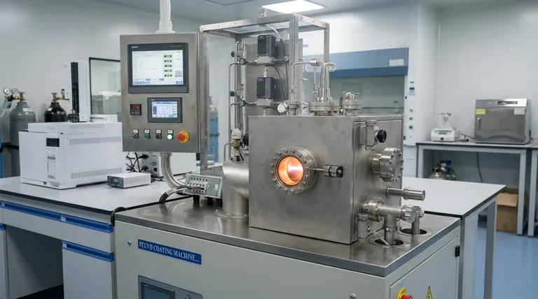
Physical Vapor Deposition encompasses processes like sputtering and thermal evaporation. In these methods, atoms are dislodged from a source material and deposited onto a substrate in a vacuum. The final thickness is a direct result of process control.
Key Factors Influencing Thickness
The most critical factor is deposition time. Longer exposure of the substrate to the vapor stream results in a thicker coating.
Another key factor is the deposition rate. This is controlled by adjusting process parameters like the power applied to the sputtering target or the temperature of the evaporation source.
Finally, the geometry and positioning of the part within the vacuum chamber affect the final thickness and its uniformity across the surface.
The Role of Thickness in Application Performance
The specified thickness is directly linked to the coating's intended function. A coating designed for one purpose may be entirely unsuitable for another.
Thin Coatings (Nanometers to ~1 µm)
Extremely thin, precise layers are often required for optical and electronic applications. For example, anti-reflective coatings on lenses or conductive layers in semiconductors are built with nanometer-scale precision.
Medium-to-Thick Coatings (~1 µm to 10+ µm)
Thicker coatings are necessary for applications demanding high wear resistance and corrosion protection. Cutting tools, engine components, and industrial molds are often coated with several microns of hard materials like Titanium Nitride (TiN) to extend their service life.
Understanding the Trade-offs and Limitations
Choosing the right thickness requires balancing performance gains with potential downsides. Simply applying a thicker coating is not always better.
Internal Stress and Adhesion
As a PVD coating gets thicker, internal stress can build up within the film. Excessive stress can lead to cracking, delamination, or peeling, causing the coating to fail entirely.
Dimensional Tolerance
Applying a coating adds material to a part's surface. For high-precision components, a thick coating can alter dimensions enough to push the part out of its required tolerance, affecting how it fits and functions in an assembly.
The PVD "Line-of-Sight" Limitation
Unlike Chemical Vapor Deposition (CVD), which has good "wrap-around" properties for complex shapes, PVD is a line-of-sight process. This can make it challenging to achieve a uniform coating thickness on intricate geometries with hidden surfaces or internal bores.
Making the Right Choice for Your Goal
Your target application dictates the ideal coating thickness. Consider the primary goal you need to achieve.
- If your primary focus is wear resistance on cutting tools or dies: A thicker coating in the 2-5 µm range is typically required to provide a durable barrier against abrasion and friction.
- If your primary focus is optical performance like anti-reflection: You need extremely thin, precisely controlled layers, often less than 100 nanometers.
- If your primary focus is corrosion protection on components: A dense, non-porous coating of 1-3 µm is often sufficient to seal the substrate from the environment.
- If your primary focus is coating a complex part with internal surfaces: You must consider if PVD's line-of-sight nature is a limitation and whether a process like CVD might be more suitable.
Ultimately, selecting the correct PVD thickness is a crucial engineering decision that directly impacts the final product's performance, reliability, and cost.
Summary Table:
| Target Application | Typical Thickness Range | Key Considerations |
|---|---|---|
| Wear Resistance (e.g., cutting tools) | ~2 - 5+ µm | Balances durability with internal stress. |
| Corrosion Protection | ~1 - 3 µm | Requires a dense, non-porous layer. |
| Optical/Electronic (e.g., AR coatings) | < 100 nm | Demands nanometer-scale precision. |
| General Functional Coatings | ~1 - 10 µm | Thickness is a primary design variable. |
Need to specify the perfect PVD coating thickness for your application?
At KINTEK, we specialize in providing the lab equipment and consumables needed to develop and test high-performance PVD coatings. Whether you're optimizing for wear resistance, corrosion protection, or specific optical properties, our solutions help you achieve precise, reliable, and cost-effective results.
Contact our experts today to discuss how we can support your laboratory's coating development and material testing needs.
Visual Guide
Related Products
- Electron Beam Evaporation Coating Oxygen-Free Copper Crucible and Evaporation Boat
- Custom CVD Diamond Coating for Lab Applications
- Round Bidirectional Press Mold for Lab
- HFCVD Machine System Equipment for Drawing Die Nano-Diamond Coating
- Molybdenum Tungsten Tantalum Special Shape Evaporation Boat
People Also Ask
- What is the temperature of e-beam evaporation? Mastering the Two-Zone Thermal Process for Precision Films
- How is an electron beam evaporator cooled during deposition? Essential Thermal Management for Stable Processes
- What is e-beam evaporation? Achieve High-Purity Thin Film Deposition for Your Lab
- What is the current of e-beam evaporation? A Guide to High-Purity Thin Film Deposition
- What is the container that holds the metal source material called in e-beam evaporation? Ensure Purity and Quality in Your Thin-Film Deposition