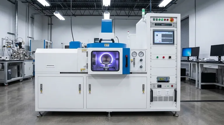
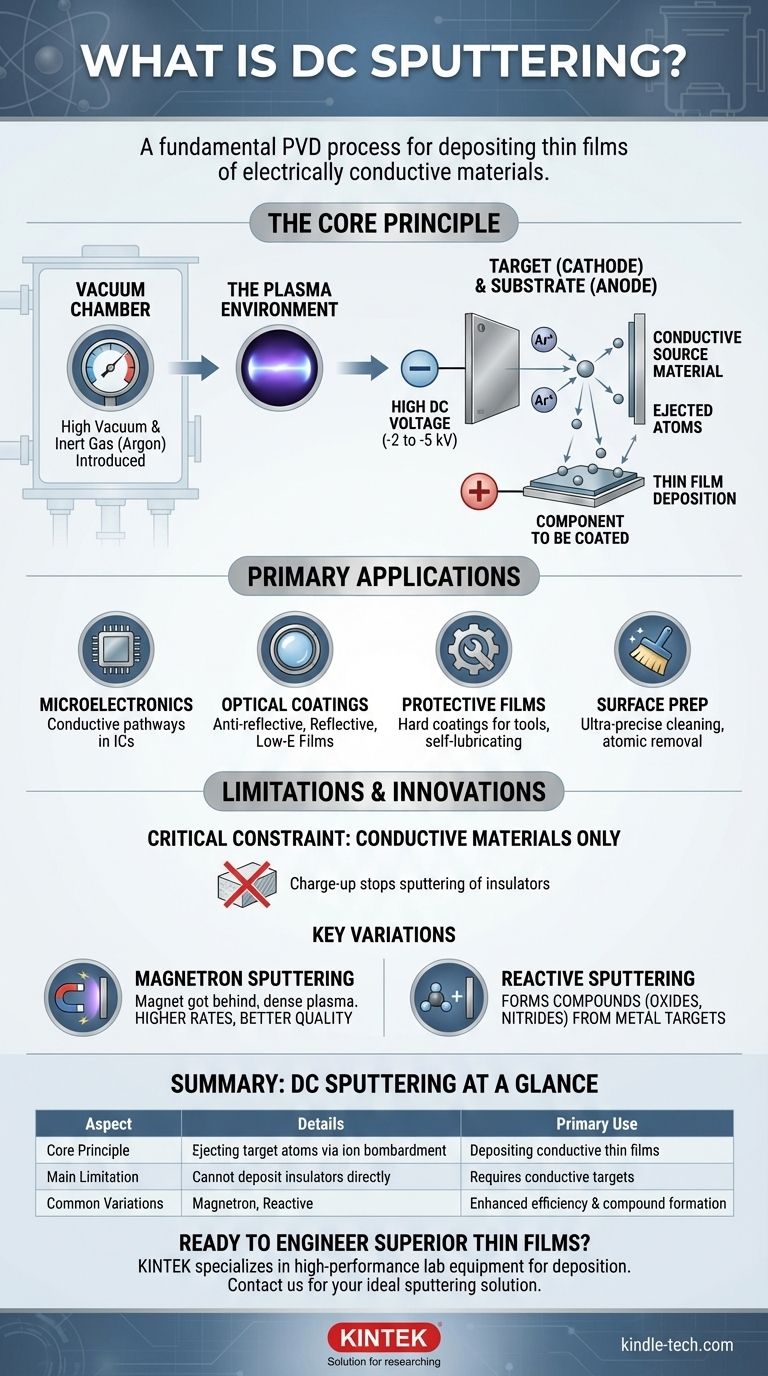
At its core, DC sputtering is a fundamental vacuum-based coating process used to deposit thin films of electrically conductive materials onto a surface. This technique, a type of physical vapor deposition (PVD), involves ejecting atoms from a source material (the "target") by bombarding it with energized gas ions. These ejected atoms then travel and settle onto a component (the "substrate"), forming a uniform layer that can be anywhere from a few nanometers to several micrometers thick.
The central purpose of DC sputtering is to create high-quality thin films of metals and other conductive materials. While it's a foundational technique, its primary limitation—the inability to deposit insulating materials—has driven the development of more advanced sputtering methods.
How DC Sputtering Works: The Core Principle
DC (Direct Current) sputtering operates on a straightforward and robust principle within a high-vacuum chamber. Understanding this process is key to appreciating its applications and limitations.
The Plasma Environment
The process begins by creating a near-vacuum and then introducing a small amount of an inert gas, typically Argon. A high DC voltage is then applied.
The Target and Substrate
A high negative voltage, usually between -2 to -5 kilovolts, is applied to the source material you wish to deposit, which is called the target. This makes the target a cathode.
The part to be coated, the substrate, faces the target and acts as the anode (the positive side of the circuit).
The Sputtering Cascade
The strong electric field strips electrons from the Argon gas atoms, creating positively charged Argon ions and a visible plasma. These positive ions are then powerfully accelerated toward the negatively charged target.
Upon impact, the ions physically knock atoms loose from the target's surface. This atomic-scale ejection is the "sputtering" effect. These freed target atoms then travel through the vacuum and deposit onto the substrate, building up a thin film one atom at a time.
Primary Applications of DC Sputtering
DC sputtering is a workhorse technology in numerous high-tech industries due to its reliability and precision.
Microelectronics and Semiconductors
Sputtering is critical for manufacturing integrated circuits. It is used to deposit the thin layers of metal, such as aluminum or copper, that form the conductive pathways connecting the billions of transistors on a chip.
Optical Coatings
The technique is widely used to create films that manage light. This includes anti-reflective coatings on lenses, reflective layers on mirrors and CDs, and films for low-emissivity glass that improves thermal insulation in buildings.
Protective and Functional Films
In the machining industry, DC magnetron sputtering is used to apply super-hard coatings to cutting tools, increasing their lifespan and performance. It is also used for creating self-lubricating films on precision components to reduce wear.
Surface Preparation and Analysis
Beyond deposition, sputtering is also used as an ultra-precise cleaning method. It can remove contaminants from a surface layer-by-layer, preparing it for subsequent high-purity processes or for chemical analysis.
Understanding the Trade-offs and Limitations
While powerful, the simplicity of DC sputtering comes with one significant constraint that defines its use case.
The Conductive Material Requirement
Standard DC sputtering only works with electrically conductive targets.
If you attempt to sputter an insulating (dielectric) material, positive charge from the impacting ions builds up on the target's surface. This "charge-up" effect eventually repels the incoming positive ions, extinguishing the plasma and stopping the sputtering process.
Deposition Rates
Compared to more advanced techniques, basic DC sputtering can have a relatively low deposition rate, which may not be suitable for high-volume manufacturing without enhancements.
Key Variations: Expanding the Capabilities
The limitations of basic DC sputtering have led to crucial innovations that are now industry standards.
Magnetron Sputtering
This is the most common evolution of DC sputtering. A powerful magnetic field is placed behind the target. This field traps electrons near the target's surface, drastically increasing the probability that they will collide with and ionize the inert gas atoms.
The result is a much denser plasma, which leads to higher sputtering rates, better film quality, and lower substrate heating. Most modern DC sputtering systems are actually DC magnetron systems.
Reactive Sputtering
This method cleverly bypasses the limitation of depositing insulators. A reactive gas, such as oxygen or nitrogen, is introduced into the vacuum chamber along with the Argon.
A conductive metal target is sputtered as usual, but the sputtered metal atoms react with the gas on their way to the substrate. For example, sputtering a silicon target in the presence of oxygen will create a silicon dioxide (an insulator) film. This allows DC power sources to create compound films like dielectrics and resistors.
Making the Right Choice for Your Goal
Your choice of sputtering technique is dictated entirely by the material you need to deposit and the performance you require.
- If your primary focus is depositing a simple, conductive metal film (like aluminum or titanium): Standard DC sputtering offers a reliable, cost-effective, and straightforward solution.
- If your primary focus is achieving higher deposition rates and better film quality for conductive materials: DC magnetron sputtering is the modern industry standard, providing superior efficiency.
- If your primary focus is depositing a compound film like an oxide, nitride, or dielectric: Reactive sputtering is the necessary technique to form these materials from a metallic target.
Understanding these core principles allows you to select the precise tool needed to engineer materials at the atomic scale.
Summary Table:
| Aspect | Details |
|---|---|
| Primary Use | Depositing thin films of conductive materials (metals) |
| Key Industries | Microelectronics, Semiconductors, Optical Coatings, Machining |
| Core Principle | Ejecting target atoms via ion bombardment in a plasma environment |
| Main Limitation | Cannot deposit insulating materials without modification |
| Common Variations | DC Magnetron Sputtering, Reactive Sputtering |
Ready to Engineer Superior Thin Films?
Whether you are developing next-generation semiconductors, precision optical coatings, or wear-resistant protective layers, choosing the right sputtering technology is critical. KINTEK specializes in providing high-performance lab equipment and consumables for all your thin-film deposition needs.
Our experts can help you select the ideal sputtering solution—from reliable DC systems for conductive metals to advanced magnetron configurations for higher efficiency.
Contact KINTALK today to discuss your project requirements and discover how our solutions can enhance your laboratory's capabilities and accelerate your research and development.
Visual Guide
Related Products
- Spark Plasma Sintering Furnace SPS Furnace
- Circulating Water Vacuum Pump for Laboratory and Industrial Use
- Multi Heating Zones CVD Tube Furnace Machine Chemical Vapor Deposition Chamber System Equipment
- Vacuum Induction Melting Spinning System Arc Melting Furnace
People Also Ask
- What technical advantages does a Spark Plasma Sintering (SPS) furnace offer for LZP ceramics? Enhance Ionic Conductivity
- What is SPS sintering method? A Guide to High-Speed, High-Performance Material Fabrication
- What are the fundamentals of spark plasma sintering process? Unlock Rapid, High-Performance Material Consolidation
- Why are Spark Plasma Sintering (SPS) furnaces or hot presses utilized in the preparation of Li3PS4 solid electrolytes?
- What is the pressure for spark plasma sintering? A Guide to Optimizing SPS Parameters


