In electronics, diamond is primarily used as a specialized semiconductor for applications that require extreme durability and performance, far exceeding the capabilities of silicon. Its main roles are in next-generation power electronics that handle immense voltage and in radiation-hardened sensors designed for harsh environments like outer space or nuclear facilities.
The key to understanding diamond's role is not seeing it as a replacement for silicon, but as a material for the extreme edge cases where silicon fails. Its unique atomic structure gives it an unmatched ability to handle high power, high temperatures, and intense radiation, making it the solution for electronics pushed to their absolute limits.
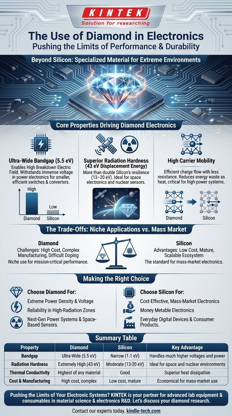
The Core Properties Driving Diamond Electronics
While silicon is the workhorse of the modern digital world, diamond is engineered for tasks that would destroy conventional electronics. This capability stems from a few fundamental physical properties.
Ultra-Wide Bandgap for High-Power Applications
A material's bandgap determines how much energy is required to make it conduct electricity. Diamond has an "ultra-wide" bandgap.
This wide bandgap gives diamond an extremely high breakdown electric field. In practical terms, this means it can withstand much higher voltages than silicon before it fails and current leaks through.
This property is the foundation for its use in power electronics, enabling the creation of smaller, more efficient, and more powerful switches and converters.
Superior Radiation Hardness
Diamond is exceptionally resistant to damage from radiation. This is measured by its displacement energy—the energy required to knock an atom out of its place in the crystal lattice.
Diamond's displacement energy is 43 eV (electron volts), more than double that of silicon, which is only 13–20 eV.
This makes it an ideal material for outer space electronics, which are constantly bombarded with cosmic rays, and for radiation sensors and dosimeters used in medical and nuclear environments.
High Carrier Mobility for Efficiency
Carrier mobility refers to how quickly charge carriers (like electrons) can move through the semiconductor material when a voltage is applied.
Diamond possesses high carrier mobility, allowing electricity to flow with less resistance.
This leads to more efficient devices that waste less energy as heat, a critical factor in high-power systems where thermal management is a primary concern.
Understanding the Trade-offs
Despite its superior properties, diamond is not poised to replace silicon in all electronics. Its adoption is limited by significant practical and economic challenges.
The Challenge of Cost and Manufacturing
Producing large, perfectly pure, single-crystal diamond wafers suitable for electronics manufacturing is an incredibly difficult and expensive process.
Silicon, by contrast, benefits from decades of optimization, making its manufacturing mature, scalable, and vastly cheaper.
Difficulties in Doping
"Doping" is the process of intentionally introducing impurities into a semiconductor to control its electrical properties. Diamond's extremely dense and rigid crystal structure makes this process much more challenging than with silicon.
This complexity can limit the types of electronic components that can be reliably fabricated using diamond.
A Niche, Not Mainstream, Material
Due to these challenges, diamond remains a niche material. It is reserved for applications where its unique performance benefits are mission-critical and justify the high cost and manufacturing complexity.
Making the Right Choice for Your Goal
The decision to use diamond is a clear trade-off between ultimate performance and practical viability.
- If your primary focus is extreme power density and voltage: Diamond is the superior choice for next-generation power systems where performance and size reduction outweigh cost.
- If your primary focus is reliability in high-radiation zones: Diamond's intrinsic hardness makes it the essential material for space-based systems and sensors in nuclear or medical settings.
- If your primary focus is cost-effective, mass-market electronics: Silicon remains the undisputed standard due to its mature manufacturing ecosystem and unparalleled economic efficiency.
Ultimately, diamond serves not as a replacement for silicon, but as a critical enabler for electronic systems that must operate far beyond conventional limits.
Summary Table:
| Property | Diamond | Silicon | Key Advantage |
|---|---|---|---|
| Bandgap | Ultra-Wide (5.5 eV) | Narrow (1.1 eV) | Handles much higher voltages and power |
| Radiation Hardness | Extremely High (43 eV) | Moderate (13-20 eV) | Ideal for space and nuclear environments |
| Thermal Conductivity | Highest of any material | Good | Superior heat dissipation |
| Cost & Manufacturing | High cost, complex | Low cost, mature | Silicon is economical for mass-market use |
Pushing the Limits of Your Electronic Systems?
Diamond semiconductors are the solution for applications where extreme performance is non-negotiable. If your research or product development requires electronics that can withstand immense power, intense radiation, or extreme temperatures, KINTEK is your partner.
We specialize in providing advanced lab equipment and consumables for cutting-edge material science and electronics R&D. Let's discuss how our solutions can help you harness the unique properties of diamond for your most demanding projects.
Contact our experts today to explore the possibilities.
Visual Guide
Related Products
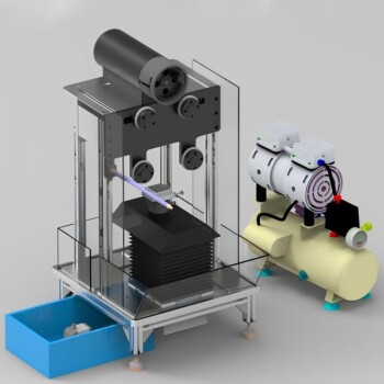
- High Precision Diamond Wire Cutting Machine Laboratory Saw Precision Wire EDM Cutting Machine
- 12 Inch 24 Inch High Precision Automatic Diamond Wire Cutting Machine Laboratory Saw Precision Wire EDM Cutting Machine
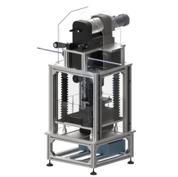
- Precision Wire Saw Laboratory Cutting Machine with 800mm x 800mm Workbench for Diamond Single Wire Circular Small Cutting
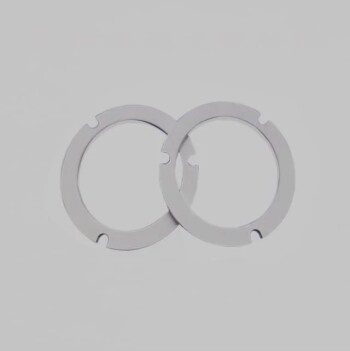
- CVD Diamond Optical Windows for Lab Applications
- CVD Diamond Domes for Industrial and Scientific Applications
People Also Ask
- How long does a diamond take to create? From Billions of Years to a Few Weeks
- How long does it take to make a diamond in a machine? From Weeks to Billions of Years
- Do natural diamonds last longer? The Truth About Diamond Durability and Value
- What machine is used for cutting diamond? Discover the Laser Technology That Shapes Gems
- Are diamonds used in machines? Unlock Superior Performance with Diamond Tools