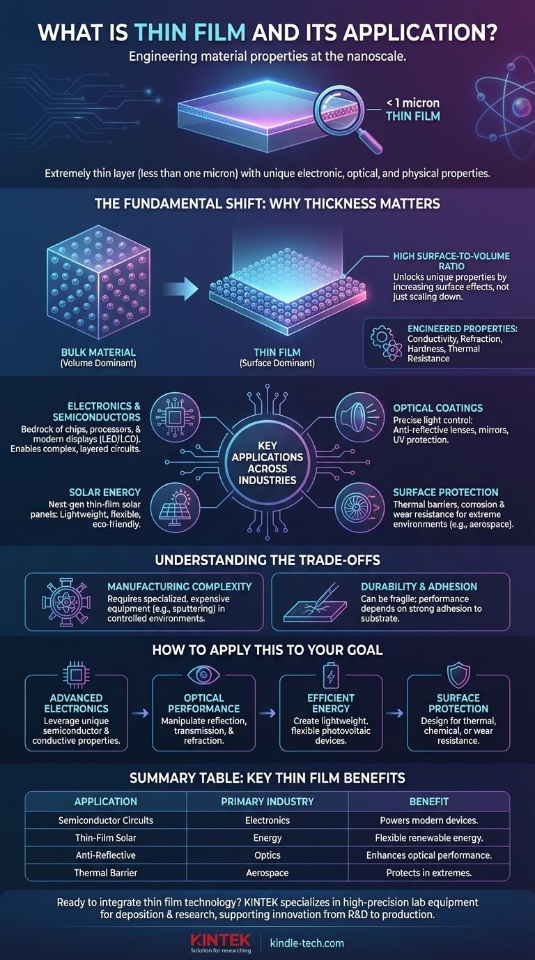
At its core, a thin film is an extremely thin layer of material, typically less than one micron thick, deposited onto a surface or substrate. These engineered layers are fundamental to modern technology, enabling everything from the anti-reflective coating on your glasses to the complex circuitry inside your smartphone and the panels in a solar farm.
The crucial insight is that materials behave differently at this microscopic scale. A thin film isn't just a smaller version of a bulk material; its high surface-to-volume ratio unlocks unique and powerful electronic, optical, and physical properties that make modern technological advancements possible.

The Fundamental Shift: Why Thickness Changes Everything
To understand the power of thin films, you must first grasp why reducing a material's dimension so drastically alters its behavior. It is not merely about making things smaller; it's about entering a new realm of material science.
The Power of the Surface-to-Volume Ratio
In any bulk material, the vast majority of atoms are on the inside, surrounded by other atoms. In a thin film, a significant percentage of atoms are on the surface or near it.
This dramatically increased surface-to-volume ratio is the key. Surface effects, which are negligible in a large block of material, become dominant and dictate the film's overall properties.
Unlocking New Material Properties
This structural change allows us to engineer properties that don't exist in the source material. We can precisely control a film's thickness and structure to manipulate its electrical conductivity, refractive index, hardness, and thermal resistance.
This is how we create materials that are transparent yet conductive, or incredibly hard yet microscopically thin.
Key Applications Across Industries
The unique properties of thin films have made them indispensable components in nearly every advanced industry, solving problems that would be impossible to address with conventional materials.
Revolutionizing Electronics and Semiconductors
Thin films are the bedrock of the entire semiconductor industry. The intricate, layered circuits within computer chips, mobile phones, and processors are built by depositing various conductive and insulating thin films.
They are also essential for modern displays, forming the active layers in LED and LCD screens that create the images we see every day.
Engineering Light with Optical Coatings
Thin films give us precise control over light. An anti-reflective coating on an optical lens is a thin film engineered to a specific thickness that cancels out light reflections.
Other optical applications include creating mirrors with enhanced reflectivity, protecting surfaces from ultraviolet radiation, and manufacturing high-refractive-index lenses.
Powering the Future with Solar Energy
The solar industry heavily relies on thin films to create a new generation of solar cells. These thin-film solar panels are often more lightweight, flexible, and ecologically friendly to produce than traditional silicon-based panels.
Their flexibility opens up possibilities for integrating solar power into unconventional surfaces, from backpacks to building facades.
Protecting Surfaces in Extreme Environments
In demanding fields like aerospace, thin films serve as protective barriers. A thermal barrier coating on a jet engine turbine blade, for example, is a thin film that protects the underlying metal from extreme temperatures.
These coatings can also provide superior resistance to corrosion and wear, significantly extending the life and reliability of critical components.
Understanding the Trade-offs
While powerful, thin film technology is not without its challenges. The process requires precision and control, and the final products have unique vulnerabilities.
Manufacturing Complexity
Depositing a uniform layer of material that is only a few atoms thick requires highly specialized and expensive equipment.
Processes like sputtering or using precursor gases must be conducted in controlled environments, such as a vacuum, to ensure the high purity and structural integrity of the film.
Durability and Adhesion
By their very nature, thin films can be fragile. Their performance is critically dependent on how well they adhere to the underlying substrate.
A microscopic scratch or a failure in adhesion can compromise the function of the entire device, whether it's an electronic circuit or a protective coating.
How to Apply This to Your Goal
The right approach to using thin film technology depends entirely on the problem you are trying to solve.
- If your primary focus is advanced electronics: Your goal is to leverage the unique semiconductor and conductive properties that only emerge at the nanoscale.
- If your primary focus is optical performance: You will be engineering film thickness and composition to precisely manipulate the reflection, transmission, and refraction of light.
- If your primary focus is efficient energy production: The key is using thin films to create lightweight, flexible, and cost-effective photovoltaic devices.
- If your primary focus is surface protection: You will be designing films to provide exceptional thermal, chemical, or wear resistance without adding significant weight or bulk.
Ultimately, thin films empower us to engineer material properties at the most fundamental level, building the foundation for the next wave of technological innovation.
Summary Table:
| Key Thin Film Application | Primary Industry Benefit |
|---|---|
| Semiconductor Circuits | Powers modern electronics and computing |
| Thin-Film Solar Panels | Enables lightweight, flexible renewable energy |
| Anti-Reflective Coatings | Enhances optical performance for lenses and displays |
| Thermal Barrier Coatings | Protects components in extreme environments like aerospace |
Ready to integrate thin film technology into your next project?
KINTEK specializes in providing the high-precision lab equipment and consumables essential for thin film deposition and research. Whether you are developing advanced semiconductors, next-generation solar cells, or durable protective coatings, our expertise supports your innovation from R&D to production.
Contact our experts today to discuss how our solutions can enhance your material engineering capabilities and help you achieve superior performance.
Visual Guide
Related Products
- Aluminized Ceramic Evaporation Boat for Thin Film Deposition
- Tungsten Evaporation Boat for Thin Film Deposition
- Electron Beam Evaporation Coating Oxygen-Free Copper Crucible and Evaporation Boat
- Molybdenum Tungsten Tantalum Evaporation Boat for High Temperature Applications
- HFCVD Machine System Equipment for Drawing Die Nano-Diamond Coating
People Also Ask
- What are thin films deposited by evaporation? A Guide to High-Purity Coating
- What is the chemical method for thin film deposition? Build Films from the Molecular Level Up
- What are the applications of thin films deposition? Unlock New Possibilities for Your Materials
- Why is an alumina boat and Ti3AlC2 powder bed necessary for Ti2AlC sintering? Protect MAX Phase Purity
- What is thin film deposition? Unlock Advanced Surface Engineering for Your Materials


